Gnss Gps - Hardware details
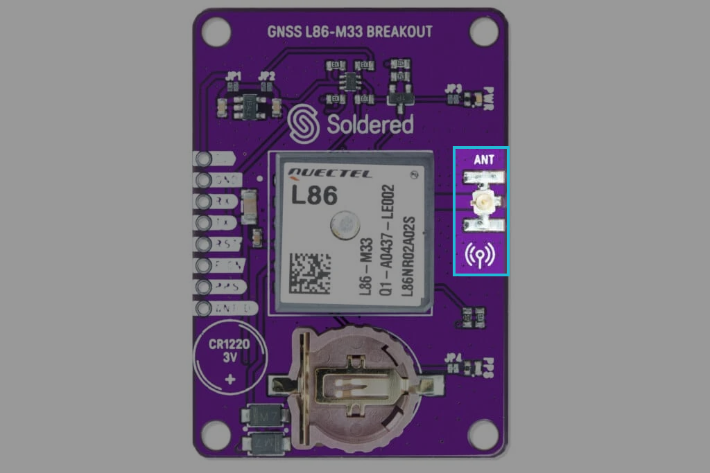
Pinout
Pin Details
| Pin Marking | Pin Name | Description |
|---|---|---|
| 5V | Power | Supply voltage. |
| GND | Ground | Common ground for power and signals. |
| RX | Receive (UART) | UART receive pin for communication. |
| TX | Transmit (UART) | UART transmit pin for communication. |
| Pin Marking | Pin Name | Description |
|---|---|---|
| RST | Reset | Resets the module when pulled low. |
| F-ON | Function On | Enables or disables the module’s function. |
| PPS | Pulse Per Second | Outputs a timing pulse per second for synchronization. |
| ANT-D | Antenna Data | Used for an external antenna connection. |
The board also features an IPX connector with SMA for an external antenna.
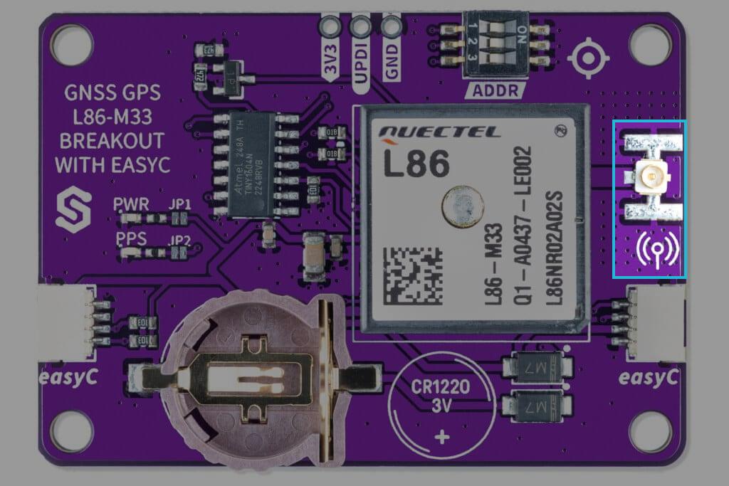
Pin Details (Qwiic version)
| Pin Marking | Pin Name | Description |
|---|---|---|
| GND | Debug Ground | Ground pin for debugging purposes. |
| UPDI | Debug Interface | Used for debugging and programming the onboard ATTiny404 microcontroller. |
| 3V3 | Debug Power | 3.3V power supply for debugging purposes. |

Qwiic (formerly easyC) details and specifications
Learn about hardware specifications, compatibility, and usage of the Qwiic connector.
Power Consumption
- Tracking Mode: Consumes approximately 26 mA at 3.3V when actively receiving signals.
- Acquisition Mode: Uses around 30 mA at 3.3V during initial satellite signal acquisition.
- Power Saving Modes:
- AlwaysLocate™ Mode: Dynamically adjusts activity to balance positioning accuracy and power consumption, reducing current usage to ~3.5 mA.
- Backup Mode: Consumes only 7 µA, preserving system data for quick restarts.
- Standby Mode: Uses around 1 mA, allowing for faster wake-ups with minimal power draw.
Dimensions
- Board Dimensions: 54mm x 38mm (2.1 x 1.5 inch)
- Header Pin Holes: 1.5 mm
- Screw Holes: Designed for M3 screws (3.2 mm diameter)
- Soldered boards are LEGO compatible! 🧱
Jumper Details
This board contains hardware jumpers. See below for their locations and functions:
| Jumper | Default State | Function |
|---|---|---|
| JP1 | NC (Normally closed) | When connected, the voltage regulator is powered by 5V, stepping it down to 3.3V for the IC. |
| JP2 | NO (Normally open) | When shorted, it bypasses the voltage regulator, allowing the board to be powered directly from 3.3V via headers. Ensure JP1 is disconnected if JP2 is connected. |
| JP3 | NC (Normally closed) | When closed, enables the PWR LED. |
| JP4 | NC (Normally closed) | When closed, enables the PPS LED. |
Jumper Details (Qwiic version)
This board contains hardware jumpers. See below for their locations and functions:
| Jumper | Default State | Function |
|---|---|---|
| JP1 | NC (Normally closed) | When closed, enables the PWR LED. |
| JP2 | NC (Normally closed) | When closed, enables the PPS LED. |
Address selection (Qwiic version)
This board contains hardware address switches. See below for how to change the breakout board's address:
| Address | SW3 | SW2 | SW1 |
|---|---|---|---|
| 0x30 | 0 | 0 | 0 |
| 0x31 | 0 | 0 | 1 |
| 0x32 | 0 | 1 | 0 |
| 0x33 | 0 | 1 | 1 |
| 0x34 | 1 | 0 | 0 |
| 0x35 | 1 | 0 | 1 |
| 0x36 | 1 | 1 | 0 |
| 0x37 | 1 | 1 | 1 |
Hardware repository
Schematics, KiCad files, Gerber files, and more can be found in the GitHub repository:
GNSS GPS L86-M33 breakout hardware design
GitHub hardware repository for this product
GNSS GPS L86-M33 breakout with easyC hardware design
GitHub hardware repository for this product
The hardware repository contains everything you need to understand, modify, or manufacture the board. The different output folders are versioned. You can check which board version you have by finding the version mark on the PCB.
Below is an overview of the available files.
CAD files
We use KiCad, an open-source PCB design tool. You can open and edit the .kicad_pro project file, which includes both the schematic and PCB layout.
The PANEL files are used internally for production.
Schematic
The OUTPUTS folder contains the schematic in .pdf format, exported from KiCad.
BOM (Bill of Materials)
The bill of materials (BOM) is provided in two formats:
- A standard
.csvtable, listing all components, part numbers, and values. - An interactive BOM (
.html) that visually highlights each component on the PCB, making it easy to locate and reference parts.
3D files
A 3D model of the PCB is available in .step format, allowing you to inspect the board design in CAD software.
Gerber files
Gerber files are essential for PCB manufacturing, as they contain precise instructions for each layer of the board. The repository includes standard Gerber outputs in a .zip file, such as:
- Copper layers (
.Cu.gbr) – Defines the traces and pads on the board. - Solder mask layers (
.Mask.gbr) – Specifies the protective solder mask. - Silkscreen layers (
.Silkscreen.gbr) – Contains text and component markings. - Paste layers (
.Paste.gbr) – Used for stencil fabrication in SMD assembly. - Drill files (
.drl) – Provides drilling coordinates for vias and holes. - Board outline (
.Edge_Cuts.gbr) – Defines the shape of the PCB. - Gerber job file (
.gbrjob) – Describes the set of Gerber files used for production.
These files are ready for fabrication and can be used in PCB manufacturing.
Compliance
The Compliance section includes important regulatory and safety documentation for this product. These files ensure compliance with relevant industry standards and legal requirements.
- CE – Certification document confirming compliance with EU safety, health, and environmental requirements.
- UKCA – UKCA (UK Conformity Assessed) certification for the UK market.
- Safety Instructions – Safety guidelines and precautions in English and in German.
- Info.txt – Contains product details such as SKU, country of origin, HS tariff code, and barcode.