Lcd I2C - Hardware details
Pinout
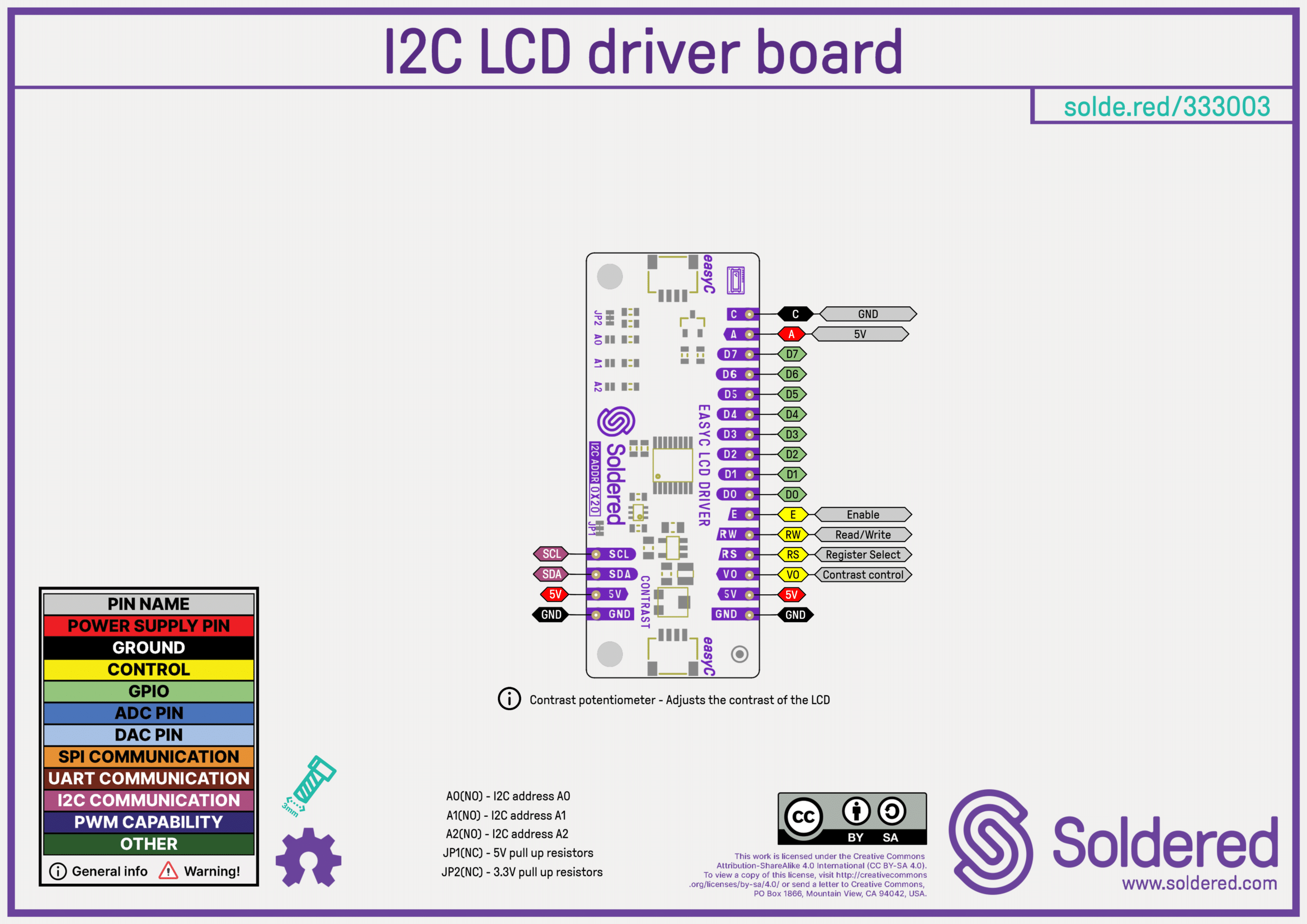
Click here for a high-resolution image of the pinout.
Pin Details
| Pin Marking | Pin Name | Description |
|---|---|---|
| SCL | Clock | I2C clock line for communication. |
| SDA | Data | I2C data line for communication. |
| 5V | Power | Supply voltage (5V). |
| A | Power | Supply voltage (5V). |
| GND | Ground | Common ground for power and signals. |
| C | Ground | Common ground for power and signals. |
| D0-D7 | Data | Values for writing or reading. |
| E | Enable | Allows or blocks the flow of data. |
| R/W | Read/Write | Selects reading or writing mode. |
| RS | Register Select | Controls where the data is written. |
| VO | Display Contrast | Controls the display contrast. |
Qwiic (formerly easyC)

Qwiic (formerly easyC) details and specifications
Learn about hardware specifications, compatibility, and usage of the Qwiic connector.
Dimensions
- Board Dimensions: 54 x 22 mm (2.1 x 0.9 inch)
- Header Pin Holes: 1.5 mm
- Screw Holes: Designed for M3 screws (3.2 mm diameter)
- LCD version:
- Display dimensions: 64.5 x 16 mm (2.5 x 0.6 inch)
- Dimensions: 80 x 36 x 12 mm (3.1 x 1.4 x 0.5 inch)
- Soldered boards are LEGO compatible! 🧱
Jumper Details
This board contains hardware jumpers; see below for their locations and functions:
| Jumper | Default State | Function |
|---|---|---|
| JP1 | NC (Normally closed) | Connects SDA/SCL pull-up resistors to 5V for I2C communication. |
| JP2 | NC (Normally closed) | Connects SDA/SCL pull-up resistors to 3.3V for I2C communication. |
Address Details
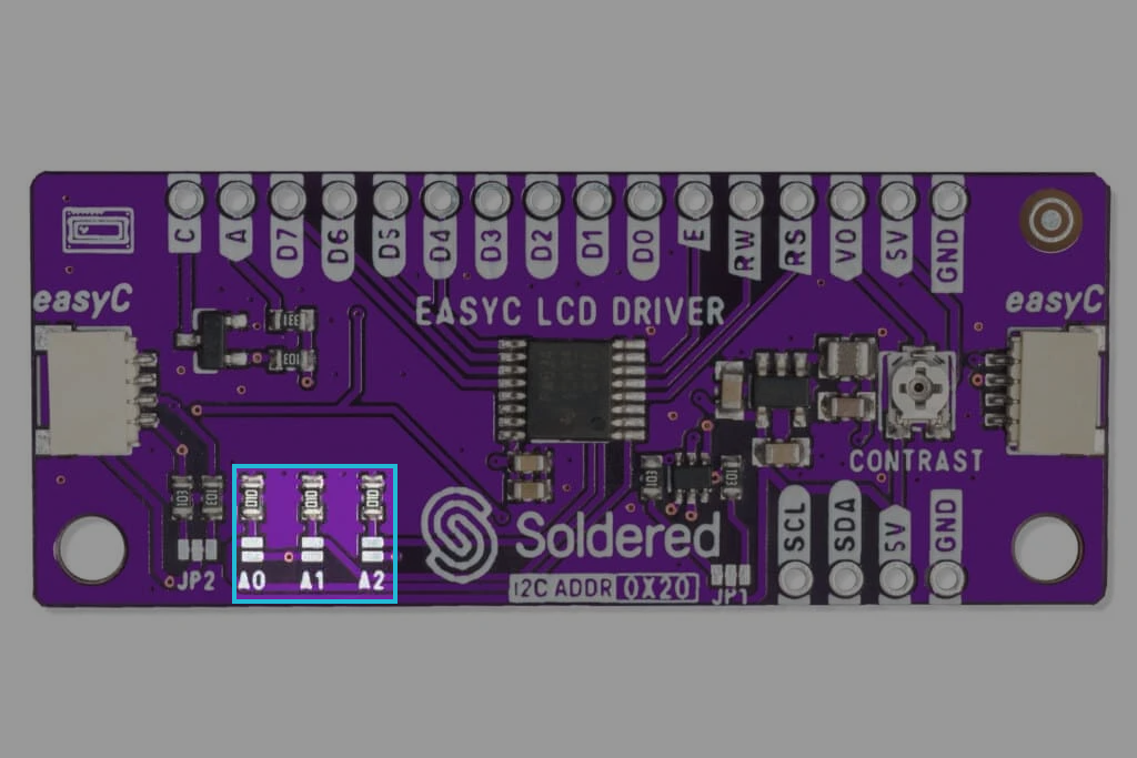
Three hardware jumpers (A0, A1, and A2) are used to program and vary the fixed I2C follower address and allow up to eight devices to share the same I2C bus or SMBus. The address can be shifted to select a unique address from 0x20 to 0x27.
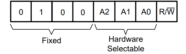
The default state of all address pins is NO (Normally opened). Closing the pins in different combinations results in different follower addresses. The value of the pin is 0 when opened and 1 when closed (see table below).
| A2 | A1 | A0 | Follower Address |
|---|---|---|---|
| 0 | 0 | 0 | 0x20 |
| 0 | 0 | 1 | 0x21 |
| 0 | 1 | 0 | 0x22 |
| 0 | 1 | 1 | 0x23 |
| 1 | 0 | 0 | 0x24 |
| 1 | 0 | 1 | 0x25 |
| 1 | 1 | 0 | 0x26 |
| 1 | 1 | 1 | 0x27 |
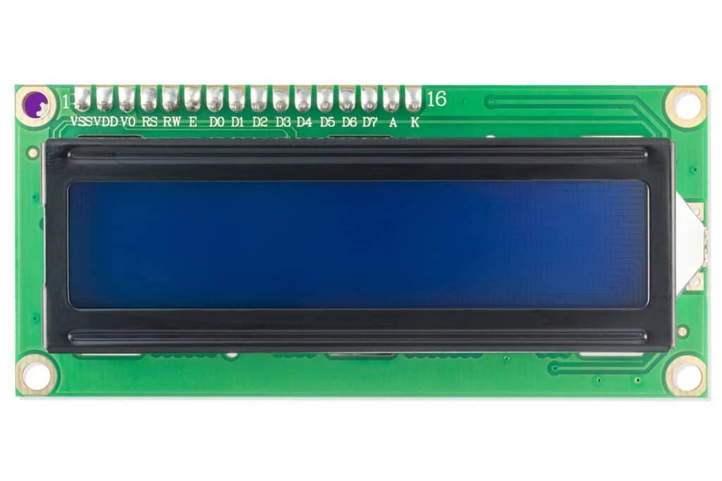
LCD Display
The version of the product with the LCD display comes with the HD44780 Dot Matrix Display Driver. It consists of two rows, and each row can print 16 characters (16x2). Each character is built using a 5x8 pixel box, resulting in a total of 1280 pixels.
Hardware repository
Schematics, KiCad files, Gerber files, and more can be found in the GitHub repository:
LCD-I2C adapter Hardware design
GitHub hardware repository for this product
The hardware repository contains everything you need to understand, modify, or manufacture the board. The different output folders are versioned. You can check which board version you have specifically by finding the version mark on the PCB.
Below is an overview of the available files.
CAD files
We use KiCad, an open-source PCB design tool. You can open and edit the .kicad_pro project file, which includes both the schematic and PCB layout.
The PANEL files are used internally for production.
Schematic
The OUTPUTS folder contains the schematic in .pdf format, exported from KiCad.
BOM (Bill of Materials)
The bill of materials (BOM) is provided in two formats:
- A standard
.csvtable, listing all components, part numbers, and values. - An interactive BOM (
.html) that visually highlights each component on the PCB, making it easy to locate and reference parts.
3D files
A 3D model of the PCB is available in .step format, allowing you to inspect the board design in CAD software.
Gerber files
Gerber files are essential for PCB manufacturing, as they contain precise instructions for each layer of the board. The repository includes standard Gerber outputs in a .zip file, such as:
- Copper layers (
.Cu.gbr) – Defines the traces and pads on the board. - Solder mask layers (
.Mask.gbr) – Specifies the protective solder mask. - Silkscreen layers (
.Silkscreen.gbr) – Contains text and component markings. - Paste layers (
.Paste.gbr) – Used for stencil fabrication in SMD assembly. - Drill files (
.drl) – Provides drilling coordinates for vias and holes. - Board outline (
.Edge_Cuts.gbr) – Defines the shape of the PCB. - Gerber job file (
.gbrjob) – Describes the set of Gerber files used for production.
These files are ready for fabrication and can be used in PCB manufacturing.
Compliance
The Compliance section includes important regulatory and safety documentation for this product. These files ensure compliance with relevant industry standards and legal requirements.
- CE – Certification document confirming compliance with EU safety, health, and environmental requirements.
- UKCA – UKCA (UK Conformity Assessed) certification for the UK market.
- Safety Instructions – Safety guidelines and precautions in English and in German.
- Info.txt – Contains product details such as SKU, country of origin, HS tariff code, and barcode.