Hardware details
Pinout
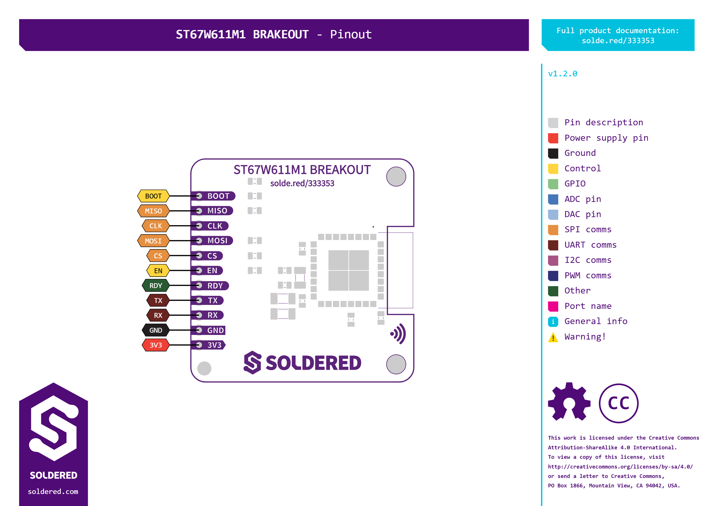
Pin Details
| Pin Marking | Pin Name | Description |
|---|---|---|
| BOOT | BOOT | Select boot from SPI or from UART. |
| MISO | Master In Slave Out | Output of SPI data from the module to the SPI master/host. |
| CLK | SPI Clock | Input of SPI clock signal generated by the SPI master/host. |
| MOSI | Master Out Slave In | Input SPI data from the master/host to the module. |
| CS | SPI Chip Select | Input of the SPI slave-select from the SPI master/host. |
| EN | Chip Enable | Chip power on. |
| RDY | SPI Ready | Data ready to be transimtted to the host processor. |
| TX | UART TX | UART TX line from ST67W611M1 point of view. |
| RX | UART RX | UART RX line from ST67W611M1 point of view. |
| GND | Ground | Common ground for power and signals. |
| 3V3 | Power | Supply voltage. |
The UART interface uses two pins (RX and TX) and is configured as follows:
- Full-duplex asynchronous communication
- Data bit lenght: 8 bits
- Stop bit lenght: 1 bit
- Parity: None
- Hardware flow control (RTS/CTS): None
- Baud rate: 2000000 bauds
- The SPI bus is configured in full-duplex slave mode with three signals: SPI_CLK, SPI_MOSI, SPI_MISO. -The SPI_RDY pin is present adns used by the ST67W611M1 as an interrupt towards the host processor.
- The SPI_CS can also be use as a wake-up signal from the host processor.
- Maximum SPI frequency: 40 MHz
Hardware repository
Schematics, KiCad files, Gerber files, and more can be found in the GitHub repository:
CAN Transceiver MCP2518 board Hardware Design
Hardware design, BOM, gerbers and 3D files for CAN-Transceiver-MCP2518-board designed by Soldered Electronics.
The hardware repository contains everything you need to understand, modify, or manufacture the board. The different output folders are versioned. You can check which board version you have by finding the version mark on the PCB.
Below is an overview of the available files.
CAD files
We use KiCad, an open-source PCB design tool. You can open and edit the .kicad_pro project file, which includes both the schematic and PCB layout.
The PANEL files are used internally for production.
Schematic
The OUTPUTS folder contains the schematic in .pdf format, exported from KiCad.
BOM (Bill of Materials)
The bill of materials (BOM) is provided in two formats:
- A standard
.csvtable, listing all components, part numbers, and values. - An interactive BOM (
.html) that visually highlights each component on the PCB, making it easy to locate and reference parts.
3D files
A 3D model of the PCB is available in .step format, allowing you to inspect the board design in CAD software.
Gerber files
Gerber files are essential for PCB manufacturing, as they contain precise instructions for each layer of the board. The repository includes standard Gerber outputs in a .zip file, such as:
- Copper layers (
.Cu.gbr) – Defines the traces and pads on the board. - Solder mask layers (
.Mask.gbr) – Specifies the protective solder mask. - Silkscreen layers (
.Silkscreen.gbr) – Contains text and component markings. - Paste layers (
.Paste.gbr) – Used for stencil fabrication in SMD assembly. - Drill files (
.drl) – Provides drilling coordinates for vias and holes. - Board outline (
.Edge_Cuts.gbr) – Defines the shape of the PCB. - Gerber job file (
.gbrjob) – Describes the set of Gerber files used for production.
These files are ready for fabrication and can be used in PCB manufacturing.
Compliance
The Compliance section includes important regulatory and safety documentation for this product. These files ensure compliance with relevant industry standards and legal requirements.
- CE – Certification document confirming compliance with EU safety, health, and environmental requirements.
- UKCA – UKCA (UK Conformity Assessed) certification for the UK market.
- Safety Instructions – Safety guidelines and precautions in English and in German.
- Info.txt – Contains product details such as SKU, country of origin, HS tariff code, and barcode.