Hardware details
Pinout
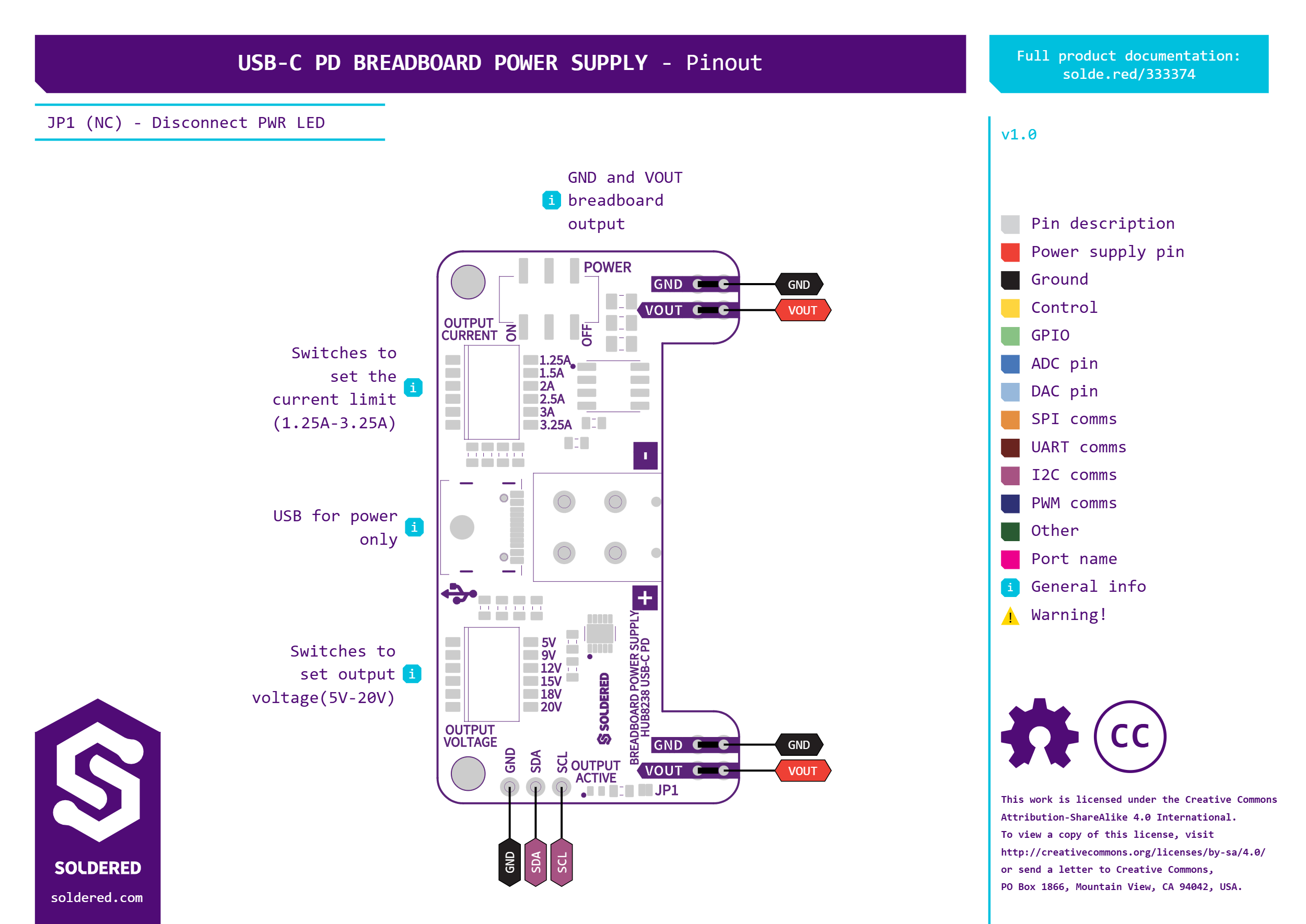
Click here for a high-resolution image of the pinout.
Pin details
| Pin Marking | Pin Name | Description |
|---|---|---|
| VOUT | Voltage Out | Negotiated output voltage supplied to the breadboard and terminal block. |
| GND | Ground | Common ground. |
| SDA | I2C Data | Optional I2C data line for dynamic configuration of the HUSB238 chip. |
| SCL | I2C Clock | Optional I2C clock line for dynamic configuration of the HUSB238 chip. |
Jumper details
| Jumper | Default State | Function |
|---|---|---|
| JP1 | NC (Normally closed) | When shorted, it provides power to the onboard power LED |
Switch details
Voltage selection switch and current selection switches control power and output:
| Switch | Function |
|---|---|
| ON/OFF Switch | Switches power to the board on or off. |
| Voltage Selection | Hardware switches used to request standard USB-PD voltage levels (5V, 9V, 12V, 15V, 20V). |
| Current Selection | Hardware switches used to set the current limit (1.25A, 1.5A, 2A, 2.5A, 3A, 3.25A). |
Dimensions
- Board Dimensions: 54 x 30mm (2.1 x 1.2 inches)
- Header Pin Holes: 1.5 mm
- Screw Holes: Designed for M3 screws (3.2 mm diameter)
- Soldered boards are LEGO-compatible! 🧱
HUSB238 USB-PD Controller
The HUSB238 is the USB Power Delivery sink controller on this board. It negotiates standard PD voltage steps and current limits from a USB-C source using hardware switch inputs, no external software or microcontroller needed.
Hardware repository
Schematics, KiCad files, Gerber files, and more can be found in the GitHub repository:
The output folders are versioned. You can find which board version you have by checking the version mark on the PCB.
CAD files
We use KiCad, an open-source PCB design tool. You can open and edit the .kicad_pcb and .kicad_sch files to inspect the board design in CAD software.
Gerber files
The repository includes standard Gerber outputs in a .zip file:
- Copper layers (
.Cu.gbr): Defines the traces and pads on the board. - Solder mask layers (
.Mask.gbr): Specifies the protective solder mask. - Silkscreen layers (
.Silkscreen.gbr): Contains text and component markings. - Paste layers (
.Paste.gbr): Used for stencil fabrication in SMD assembly. - Drill files (
.drl): Provides drilling coordinates for vias and holes. - Board outline (
.Edge_Cuts.gbr): Defines the shape of the PCB. - Gerber job file (
.gbrjob): Describes the set of Gerber files used for production.
Compliance
Regulatory and safety documents for this product:
- CE: Certification document confirming compliance with EU safety, health, and environmental requirements.
- UKCA: UKCA (UK Conformity Assessed) certification for the UK market.
- Safety Instructions: Safety guidelines and precautions provided in English and German.
- Info.txt: Contains product details such as SKU, country of origin, HS tariff code, and barcode.