P82B715 I2C Bus Extender - How it works
The P82B715 I2C Bus Extender breakout board extends the range of standard I²C communication far beyond its usual limits. At its core is the P82B715 chip by NXP/Texas Instruments, a bidirectional I²C bus buffer that drives 10× lower-impedance bus wiring. Each side is buffered from the other, so the long cable's capacitance never reaches your microcontroller's bus and I²C signals can travel over twisted-pair runs of up to 50 meters.
Datasheet
For an in-depth look at technical specifications, refer to the official P82B715 datasheet:
P82B715 Datasheet (TI)
Detailed technical documentation for the P82B715 I²C bus extender chip.
I²C bus limitations
Standard I²C has a maximum bus capacitance of 400 pF, which limits usable cable length to only a few meters. As capacitance increases, signal rise times slow down and communication becomes unreliable or fails entirely.
The P82B715 solves this by isolating the local side from the extended side. Each side is driven independently, so the capacitive load of the long cable does not affect the microcontroller's I²C bus.
Bidirectional buffering
The P82B715 operates as a transparent, bidirectional buffer:
- Local side (Sx/Sy): Runs at 5V. It goes straight to header K3, and reaches the Qwiic ports (K1/K2) through an onboard level shifter that converts it to 3.3V. Supports up to 400 pF bus capacitance.
- Extended side (Lx/Ly): Connects to the screw terminal (K4) for the long cable run. Also 5V, supports up to 3000 pF bus capacitance and runs of up to 50 m.
The chip is completely invisible to the I²C protocol. It adds no address, register, or configuration layer, so the microcontroller communicates directly with remote devices using their original I²C addresses.
The chip keeps all the normal I²C operating modes. In practice, use Standard-mode (100 kHz) for long runs and save faster clocks for short, well behaved cable.
Onboard signal chain
This breakout board adds supporting components around the P82B715:
- Boost converter (TPS613222A): Steps up the 3.3V Qwiic supply to 5V, powering the P82B715 chip and the fixed 5V pull-ups on the extended side.
- Level shifter (dual NMOS): Sits between the Qwiic connectors and the P82B715's Sx/Sy pins, translating between 3.3V and 5V in both directions. It is always in circuit.
So your microcontroller sees 3.3V I²C on the Qwiic side, while header K3, the P82B715 and the screw terminal all sit at 5V.
Pull-up resistors
I²C's SDA and SCL lines are open-drain: a device can only pull a line low, never drive it high. Pull-up resistors are what bring the line back to a logic high when nothing's pulling it down, as shown below for a typical controller/peripheral pair.
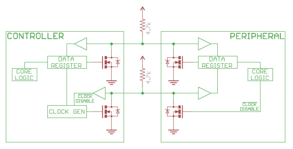
The resistor value matters: too high and rise times get too slow for reliable communication as bus capacitance increases (exactly the problem the P82B715 is built to work around), too low and it wastes power and can't be pulled fully low by the sinking device. This board provides pull-ups differently on each side:
- Extended side (Lx/Ly, screw terminal K4): Fixed 470 Ω pull-ups to 5V, always active. There's no jumper for these.
- Local side: 10 kΩ pull-ups, enabled per voltage domain rather than per line:
- JP1 ties the 5V rail to the pull-ups on the 5V nets, the ones shared by the P82B715's Sx/Sy pins and header K3.
- JP2 ties the 3V3 rail to the pull-ups on the Qwiic side of the level shifter.
Both are SMD jumpers with a centre pad on the rail and one trace out to each line, closed from the factory. Cut one trace to drop the pull-up on just that line, or both to drop the pair. Do that when the device on that side already brings its own pull-ups, so the resistors don't end up in parallel.