SCD43 - Hardware details
Pinout
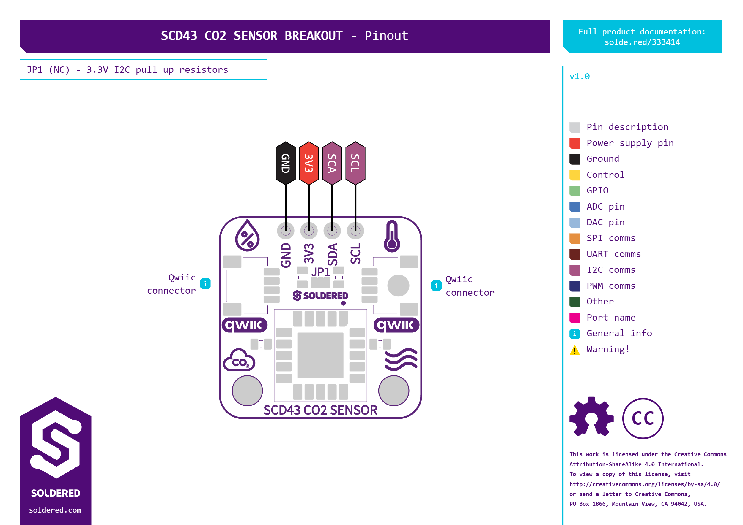
Click here for a high-resolution image of the pinout.
Pin details
| Pin Marking | Pin Name | Description |
|---|---|---|
| GND | Ground | Common ground for power and signals. |
| VCC | Power | Supply voltage (both 5V and 3V3 are supported). |
| SDA | Data | I2C data line for communication. |
| SCL | Clock | I2C clock line for communication. |
Qwiic (formerly easyC)

Qwiic (formerly easyC) details and specifications
Learn about hardware specifications, compatibility, and usage of the Qwiic connector.
Dimensions
- Board Dimensions: 22 × 22 mm (0.9 × 0.9 inch)
- Header Pin Holes: 1.0 mm
- Screw Holes: Designed for M3 screws (3.2 mm diameter)
- Soldered boards are LEGO compatible! 🧱
Jumper Details
This board contains hardware jumpers, see below for their locations and functions:
| Jumper | Default State | Function |
|---|---|---|
| JP1 | NC (Normally closed) | Connects the I2C SDA/SCL pull-up resistors. Cut to disable pull-ups if they conflict with other devices on the bus. |
Hardware repository
The hardware repository contains everything you need to understand, modify, or manufacture the board. The different output folders are versioned. You can check which board version you have specifically by finding the version mark on the PCB.
Below is an overview of the available files.
CAD files
We use KiCad, an open-source PCB design tool. You can open and edit the .kicad_pro project file, which includes both the schematic and PCB layout.
The PANEL files are used internally for production.
Schematic
The OUTPUTS folder contains the schematic in .pdf format, exported from KiCad.
BOM (Bill of Materials)
The bill of materials (BOM) is provided in two formats:
- A standard
.csvtable, listing all components, part numbers, and values. - An interactive BOM (
.html) that visually highlights each component on the PCB, making it easy to locate and reference parts.
3D files
A 3D model of the PCB is available in .step format, allowing you to inspect the board design in CAD software.
Gerber files
Gerber files are essential for PCB manufacturing, as they contain precise instructions for each layer of the board. The repository includes standard Gerber outputs in a .zip file, such as:
- Copper layers (
.Cu.gbr) - Defines the traces and pads on the board. - Solder mask layers (
.Mask.gbr) - Specifies the protective solder mask. - Silkscreen layers (
.Silkscreen.gbr) - Contains text and component markings. - Paste layers (
.Paste.gbr) - Used for stencil fabrication in SMD assembly. - Drill files (
.drl) - Provides drilling coordinates for vias and holes. - Board outline (
.Edge_Cuts.gbr) - Defines the shape of the PCB. - Gerber job file (
.gbrjob) - Describes the set of Gerber files used for production.
These files are ready for fabrication and can be used in PCB manufacturing.
Compliance
The Compliance section includes important regulatory and safety documentation for this product. These files ensure compliance with relevant industry standards and legal requirements.
- CE - Certification document confirming compliance with EU safety, health, and environmental requirements.
- UKCA - UKCA (UK Conformity Assessed) certification for the UK market.
- Safety Instructions - Safety guidelines and precautions in English and in German.
- Info.txt - Contains product details such as SKU, country of origin, HS tariff code, and barcode.