BHI385 Smart IMU - Hardware details
Pinout
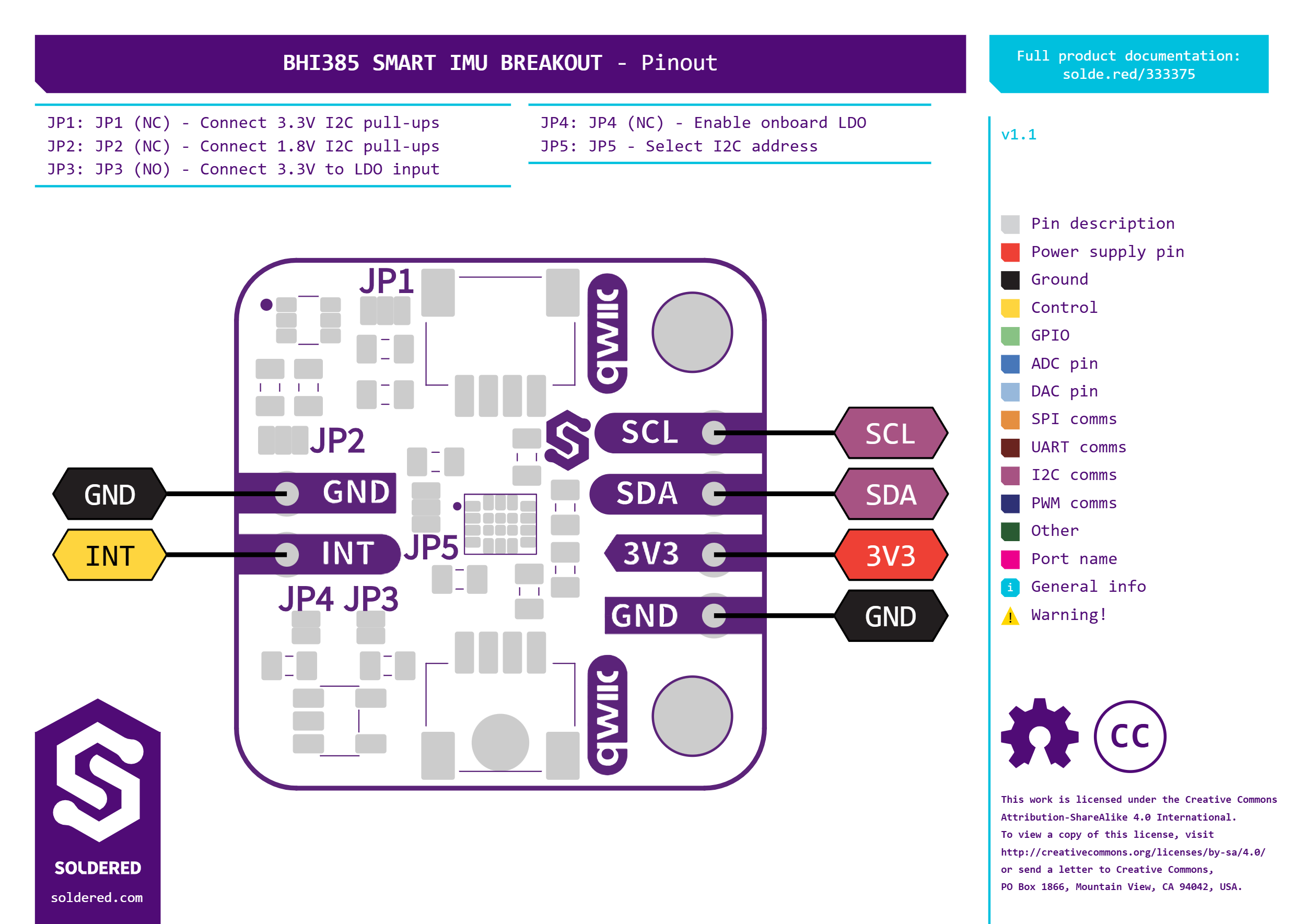
Pin details
| Pin Marking | Pin Name | Description |
|---|---|---|
| INT | Interrupt | Active interrupt output from the BHI385 HIRQ pin (3.3V logic) |
| GND | Ground | Common ground for power and signals |
| 3V3 | Power | 3.3V supply input |
| SCL | Clock | I2C clock line (3.3V level, level-shifted to 1.8V on board) |
| SDA | Data | I2C data line (3.3V level, level-shifted to 1.8V on board) |
Qwiic (formerly easyC)

Qwiic (formerly easyC) details and specifications
Learn about hardware specifications, compatibility, and usage of the Qwiic connector.
Dimensions
- Board Dimensions: 22 × 22 mm (0.87 × 0.87 in)
- Header Pin Holes: 1.5 mm
- Screw Holes: Designed for M3 screws (3.2 mm diameter)
- Soldered boards are LEGO compatible! 🧱
Jumper Details
This board contains hardware jumpers; see below for their locations and functions:
| Jumper | Default State | Function |
|---|---|---|
| JP1 | NC (Normally closed) | Connects the 3.3V-side pull-up resistors (both SDA and SCL) on the I2C level-shifter to the 3V3 rail. |
| JP2 | NC (Normally closed) | Connects the 1.8V-side pull-up resistors (both SDA and SCL) on the I2C level-shifter to the 1.8V rail. |
| JP3 | NO (Normally open) | Connects the 3.3V rail to the input of the onboard LDO regulator. Bridge to power the LDO from 3V3; leave open to isolate the regulator input. |
| JP4 | NC (Normally closed) | Connects the EN pin of the onboard regulator to the 3.3V rail, enabling the regulator. |
| JP5 | 0x29 | Selects the I2C address: bridge towards 0x29 (HSDO = VDDIO, default) or 0x28 (HSDO = GND). |
Hardware repository
The hardware repository contains everything you need to understand, modify, or manufacture the board. The different output folders are versioned. You can check which board version you have specifically by finding the version mark on the PCB.
Below is an overview of the available files.
CAD files
We use KiCad, an open-source PCB design tool. You can open and edit the .kicad_pro project file,
which includes both the schematic and PCB layout.
The PANEL files are used internally for production.
Schematic
The OUTPUTS folder contains the schematic in .pdf format, exported from KiCad.
BOM (Bill of Materials)
The bill of materials (BOM) is provided in two formats:
- A standard
.csvtable, listing all components, part numbers, and values. - An interactive BOM (
.html) that visually highlights each component on the PCB, making it easy to locate and reference parts.
3D files
A 3D model of the PCB is available in .step format, allowing you to inspect the board design
in CAD software.
Gerber files
Gerber files are essential for PCB manufacturing. The repository includes copper layers, solder mask, silkscreen, paste layers, drill files, board outline, and the Gerber job file.
Compliance
The Compliance section includes CE, UKCA, Safety Instructions, and an Info.txt file.