Inkplate 5V2 – Hardware files
The hardware files for Inkplate 5V2 live in the repository below:
Soldered Inkplate 5V2 hardware design
Hardware design, BOM, gerbers, and 3D files for Soldered Inkplate 5V2, designed by Soldered Electronics
Repository contents
The Inkplate 5V2 hardware repository holds what you need to understand, modify, or manufacture the board. Here's an overview of the files:
CAD files
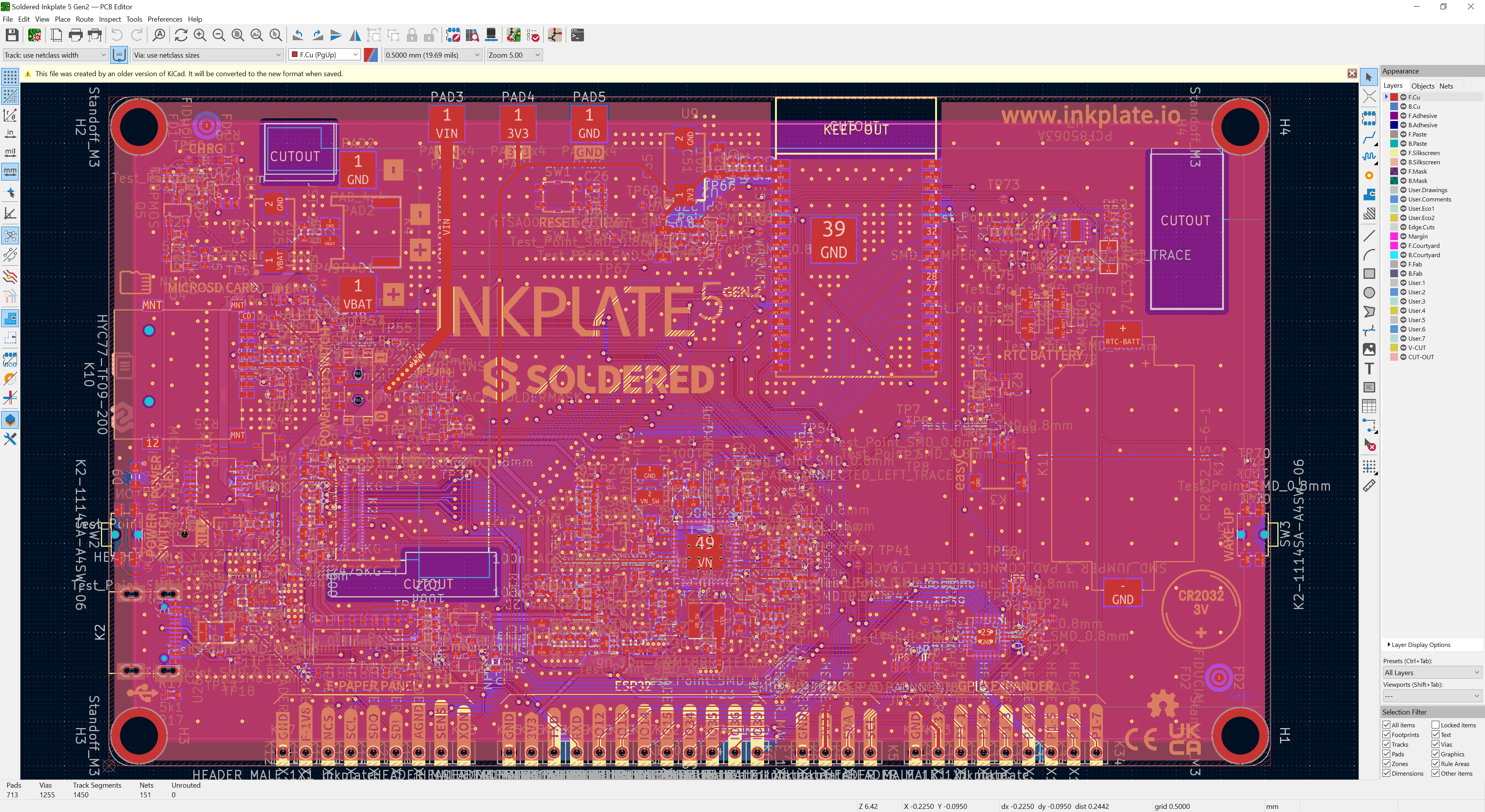
We use KiCad, an open-source PCB design tool. You can open and edit the .kicad_pro project file, which includes both the schematic and the PCB layout.
The PANEL files are used internally for production.
Schematic
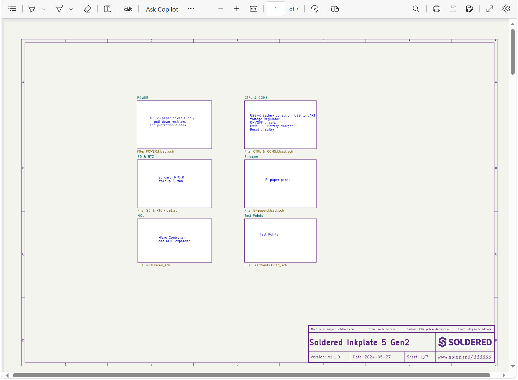
The OUTPUTS folder contains the schematic in .pdf format, exported from KiCad. It's split into sections by functionality, so it's easy to navigate.
BOM (Bill of Materials)
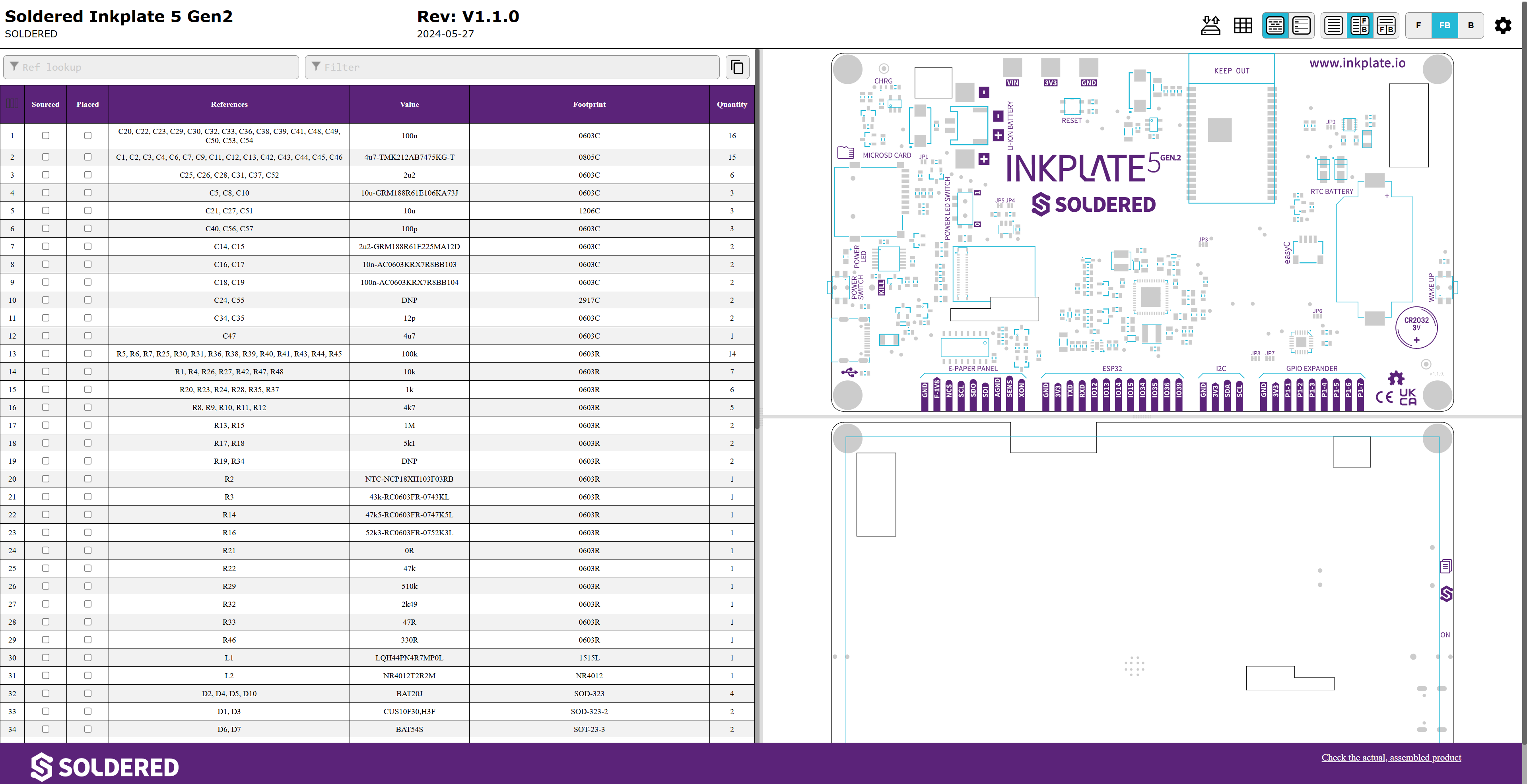
The bill of materials (BOM) is provided in two formats:
- A standard
.csvtable, listing all components, part numbers, and values. - An interactive BOM (
.html) that highlights each component on the PCB, so parts are easy to locate and reference.
3D files
A 3D model of the PCB is available in .step format, so you can inspect the board design in CAD software.
Gerber files
Gerber files carry the precise instructions for each layer of the board, which is what a PCB manufacturer needs. The repository includes the standard Gerber outputs in a .zip file:
| File | What it holds |
|---|---|
Copper layers (.Cu.gbr) | The traces and pads on the board. |
Solder mask layers (.Mask.gbr) | The protective solder mask. |
Silkscreen layers (.Silkscreen.gbr) | Text and component markings. |
Paste layers (.Paste.gbr) | Used for stencil fabrication in SMD assembly. |
Drill files (.drl) | Drilling coordinates for vias and holes. |
Board outline (.Edge_Cuts.gbr) | The shape of the PCB. |
Gerber job file (.gbrjob) | A description of the set of Gerber files used for production. |
These files are ready to send straight to a PCB manufacturer.