7.5 Shift Register
Every pin on the board is spoken for eventually. This project shows how to get more outputs than you have pins: a 74HC595 shift register turns three pins into eight, and we use four of them to build a counter that counts from 0 to 15 in binary, the way a computer does.
In this documentation you will learn:
- How a 74HC595 shift register turns three pins into eight outputs
- What shifting and latching mean, and why the LEDs all change at the same instant
- How to write your own
shift_out()with the bit shift and bitwise AND operators - How to seat a 16-pin chip on a breadboard without getting it backwards
- How to read a binary number off a row of LEDs
Hardware required
- 1x Soldered NULA MINI board
- 1x Breadboard
- 1x 74HC595 shift register
- 4x LEDs
- 4x 330 Ω resistors
- 14x Jumper wires
- 1x USB-C cable
Putting the components together
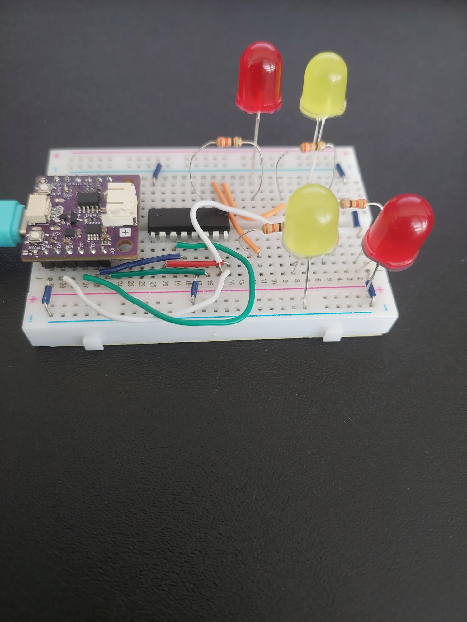
This build has more connections than anything else in the kit, so it is worth going slowly. Every photo below is the board after one more thing went in, twenty-one steps in all: fourteen jumper wires, four resistors, four LEDs and the chip.
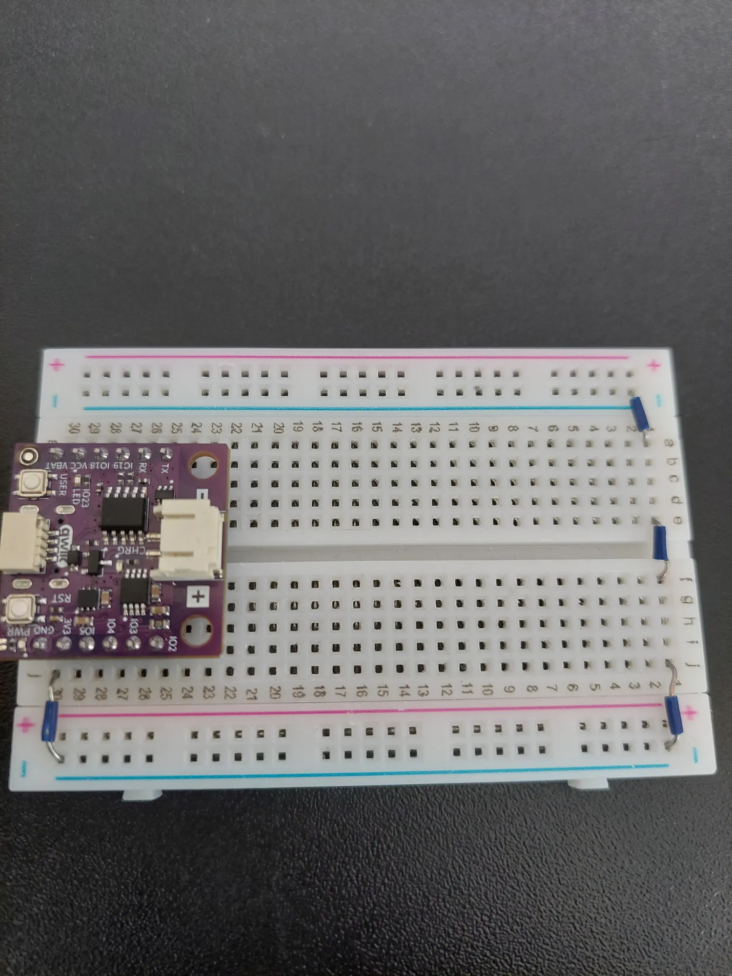
1. Insert the board and build the ground rail
Push the NULA MINI into one end of the breadboard so it occupies rows 25 to 30, then build the shared ground before anything else. This is the first example that needs ground on both sides of the board, and the two blue − rails along the edges are not joined to each other inside the breadboard.
They are also too far apart to reach with one jumper, so the connection is made in hops, using row 1 as a stepping stone:
j30(GND) to the bottom blue−rail- the bottom blue
−rail toj1 e1tof1, crossing the centre channela1to the top blue−rail
After those four jumpers, both rails and both halves of row 1 are one single ground.
2. Press in the 74HC595
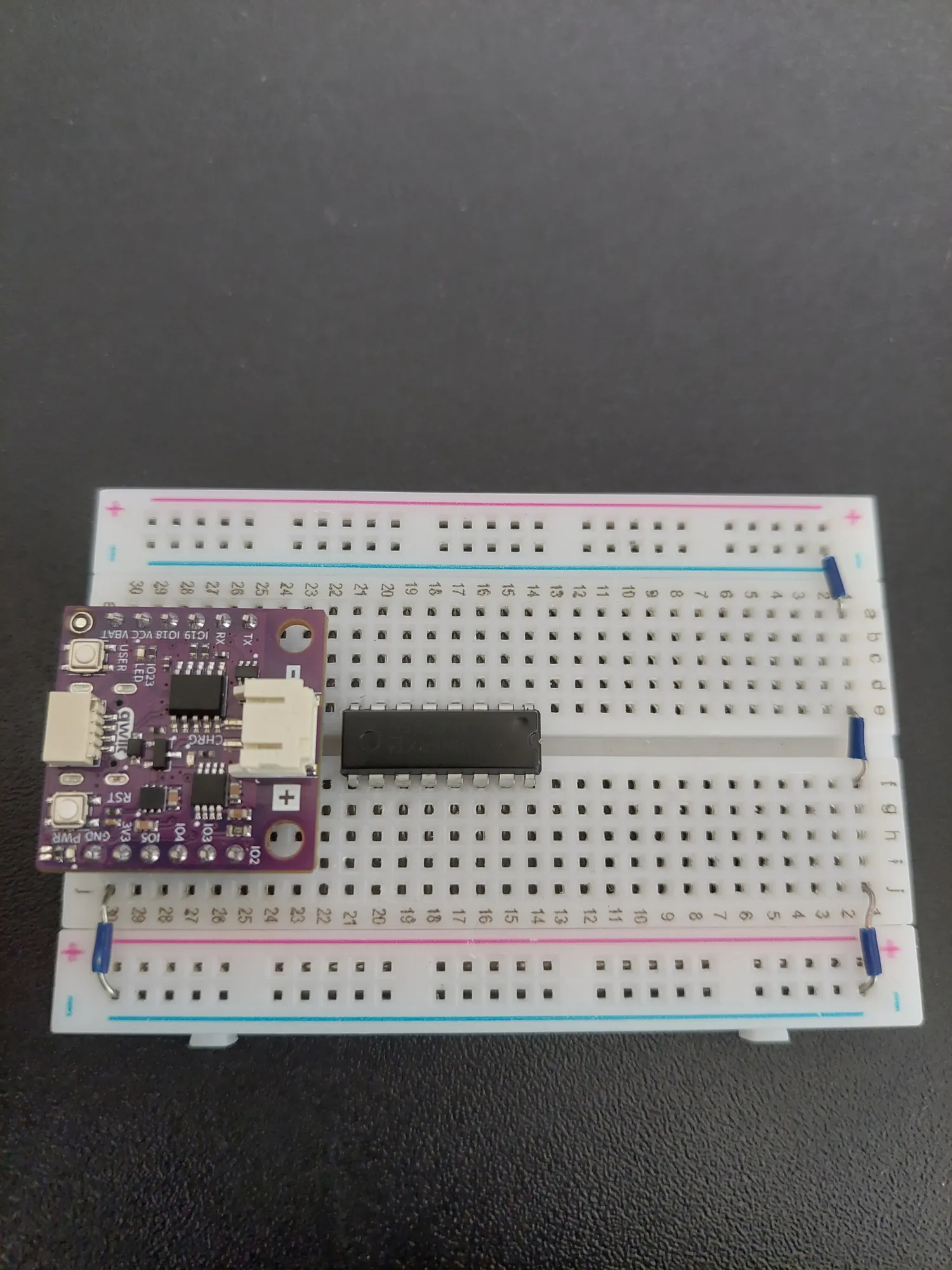
The chip straddles the centre channel and occupies rows 14 to 21, with the half-moon notch facing row 14, away from the board. One row of pins lands in column e, the other in column f.
With the notch at row 14, the pins sit like this:
| Row | 14 | 15 | 16 | 17 | 18 | 19 | 20 | 21 |
|---|---|---|---|---|---|---|---|---|
| a–e side | 1 · Q1 | 2 · Q2 | 3 · Q3 | 4 · Q4 | 5 · Q5 | 6 · Q6 | 7 · Q7 | 8 · GND |
| f–j side | 16 · VCC | 15 · Q0 | 14 · DS | 13 · OE | 12 · ST_CP | 11 · SH_CP | 10 · MR | 9 · Q7' |
3. Ground the chip
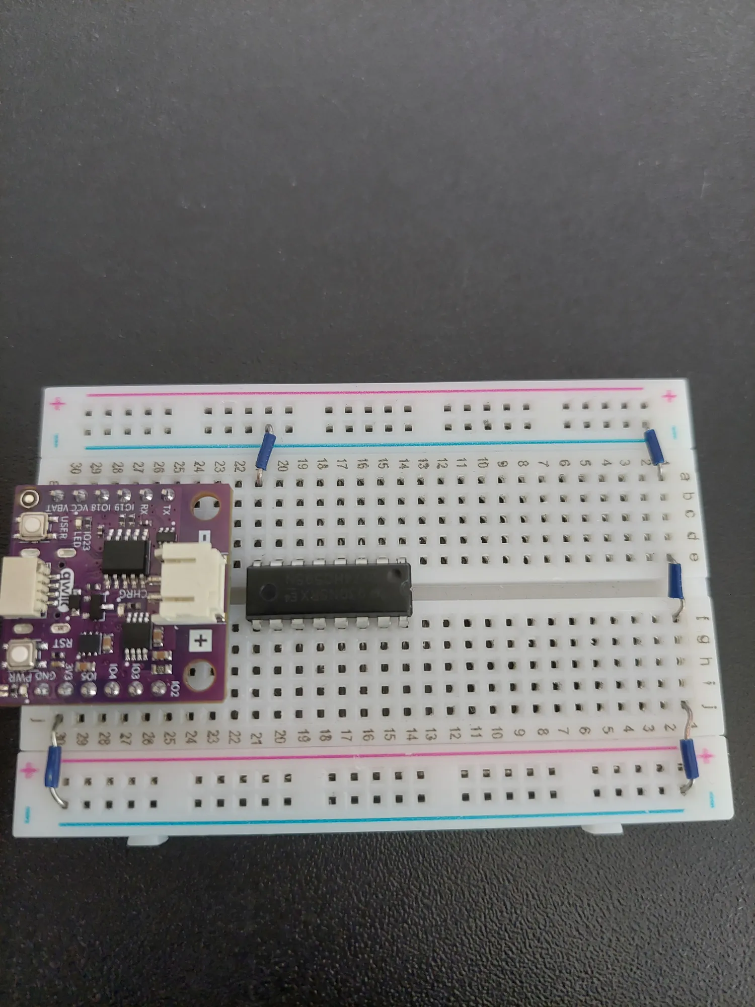
A short blue jumper takes pin 8 from a21 to the top blue − rail.
4. Give the chip power
The white wire carries 3V3 from j29 to j14, the VCC pin of the chip. It loops down below the board rather than crossing straight over, because that is the length of wire that was to hand. Nothing is connected underneath.
VCC pin of the board. VCC is the 5 V arriving over USB, and a 74HC595 powered at 5 V needs 3.5 V to recognise a high, more than the 3.3 V pins of the board can produce. It would work on the bench and fail somewhere else.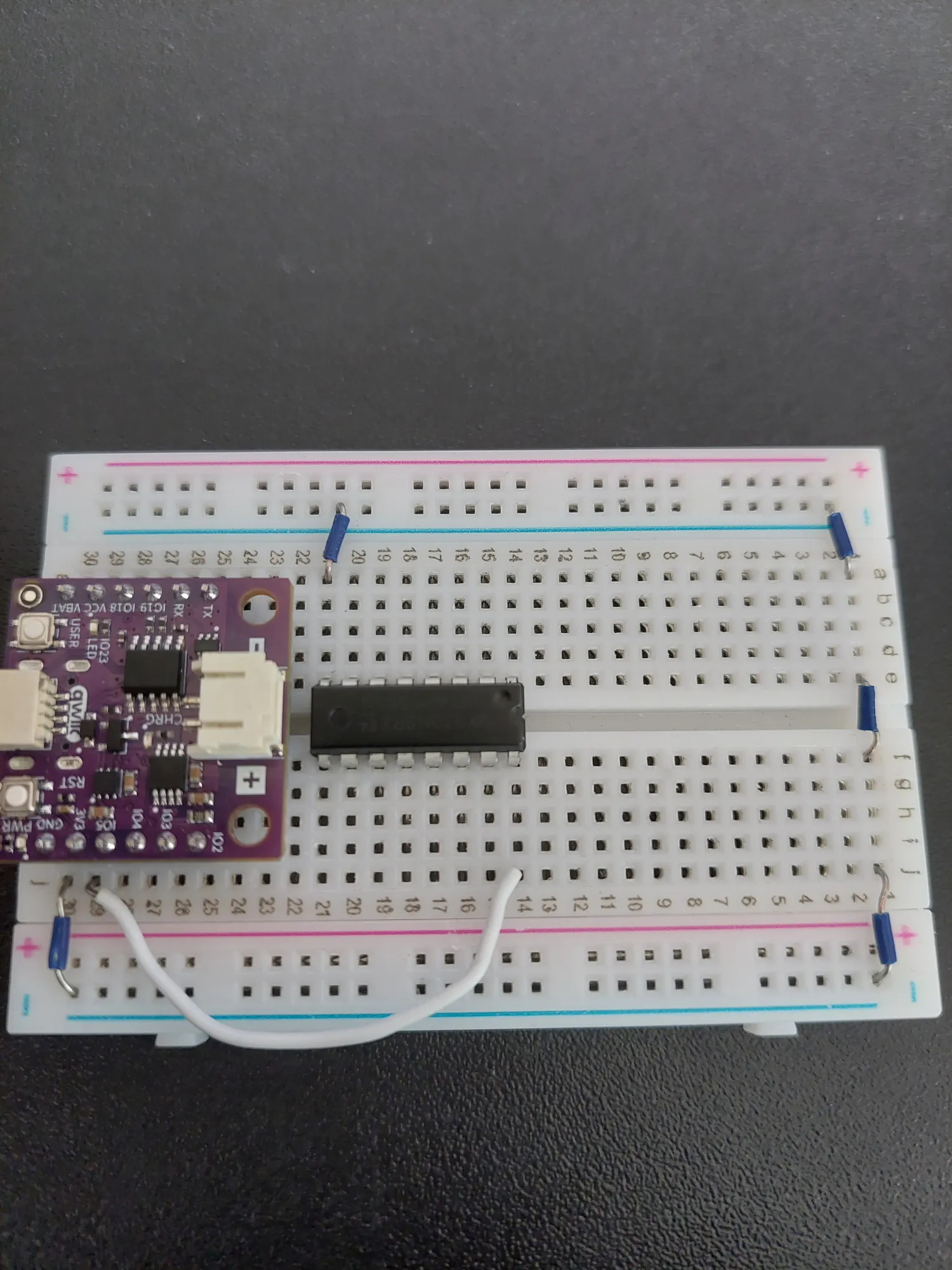
5. Tie Master Reset high
The red wire runs i20 to i14, pin 10 (MR) across to pin 16 (VCC). MR wipes the whole register whenever it is low, so it has to be held high, and the nearest high is the supply pin you just connected.
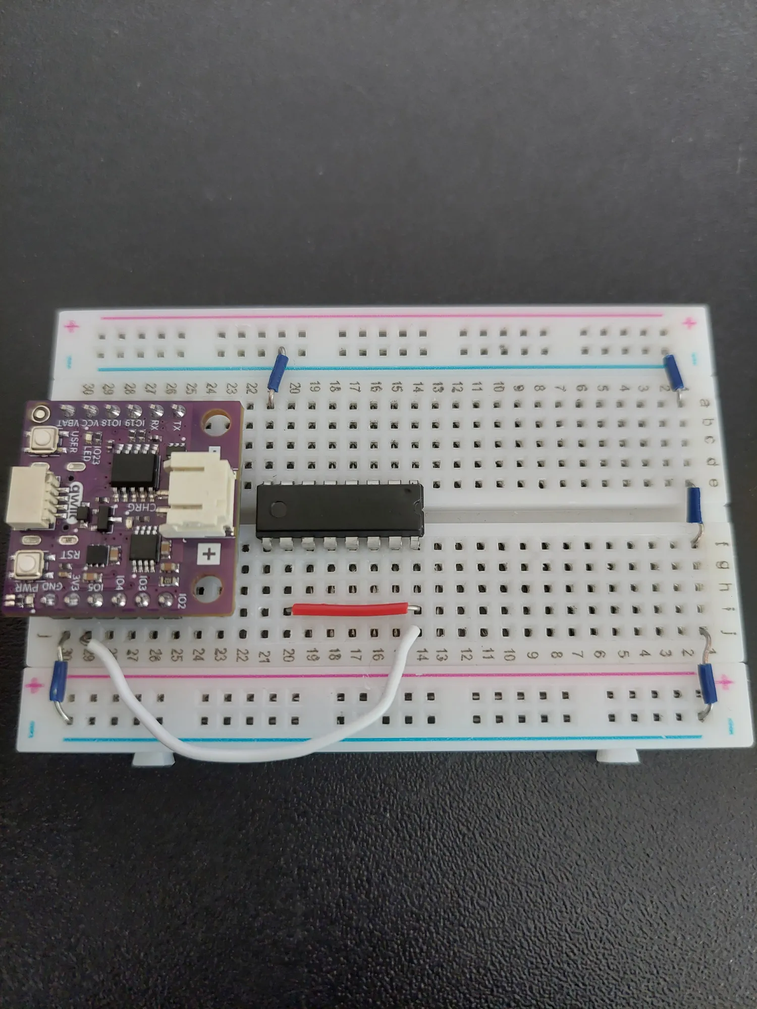
6. Enable the outputs
A second short blue jumper takes j17 (pin 13, OE) down to the bottom blue − rail. Output Enable disconnects all eight outputs whenever it is high, so it has to be held low.
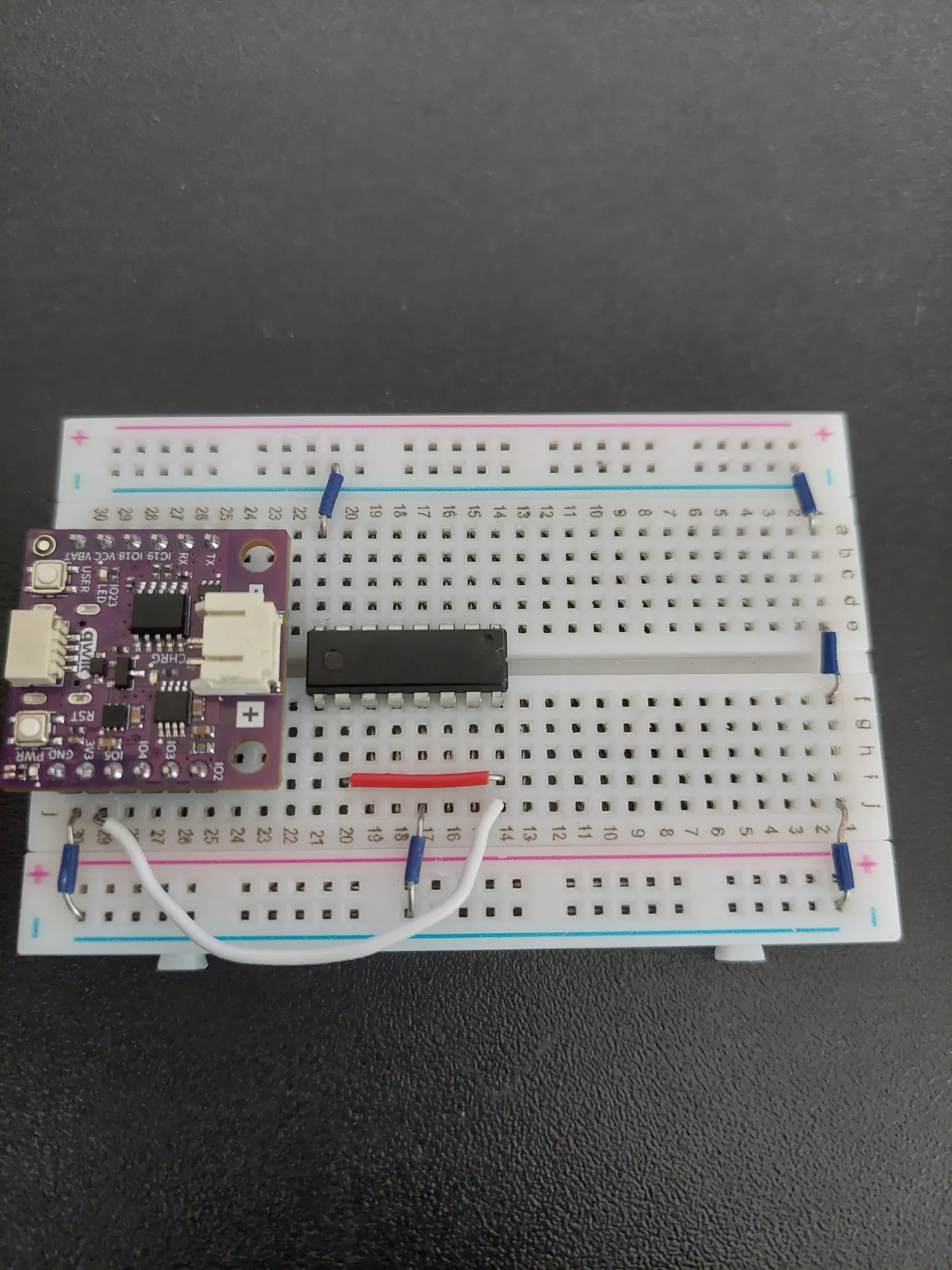
7. Connect the data line
The dark green wire runs j25 (IO2) to j16, pin 14, DS. This is the pin the bits themselves travel over, one after another.
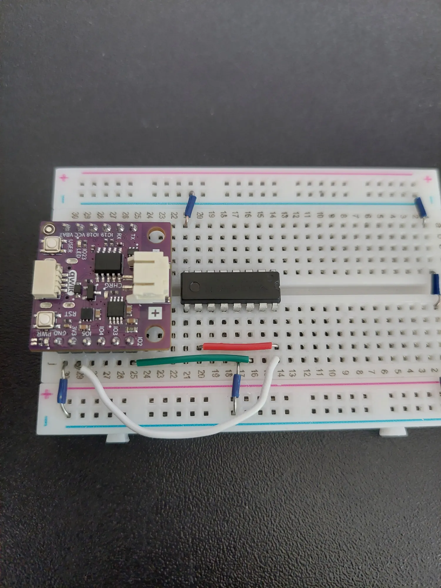
8. Connect the latch
The dark blue wire runs j26 (IO3) to h18, pin 12, ST_CP. This is the one that makes all eight outputs change together instead of flickering through every step.
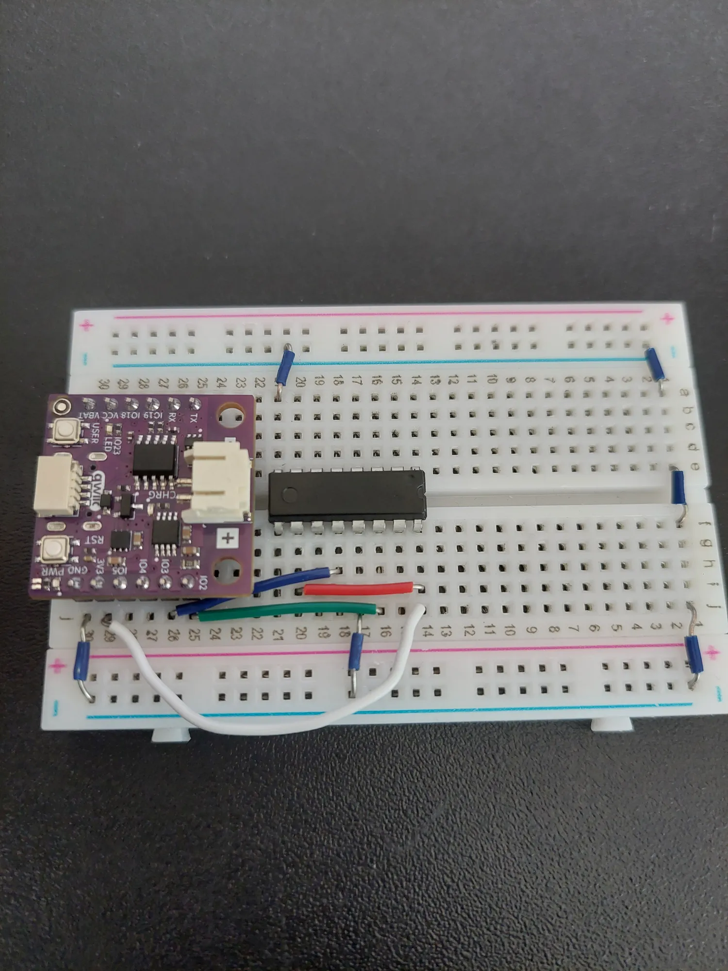
9. Connect the clock
The teal wire runs j27 (IO4) to g19, pin 11, SH_CP. Like the power wire it takes the long way round below the board.
That completes the wiring of the chip:
| Wire | From | To | Chip pin | Why |
|---|---|---|---|---|
| Blue (short) | a21 | top − rail | 8 · GND | Chip ground |
| White | j29 (3V3) | j14 | 16 · VCC | Chip power |
| Red | i20 | i14 | 10 · MR to VCC | Master Reset held high |
| Blue (short) | j17 | bottom − rail | 13 · OE | Output Enable held low |
| Dark green | j25 (IO2) | j16 | 14 · DS | Data |
| Dark blue | j26 (IO3) | h18 | 12 · ST_CP | Latch |
| Teal | j27 (IO4) | g19 | 11 · SH_CP | Clock |
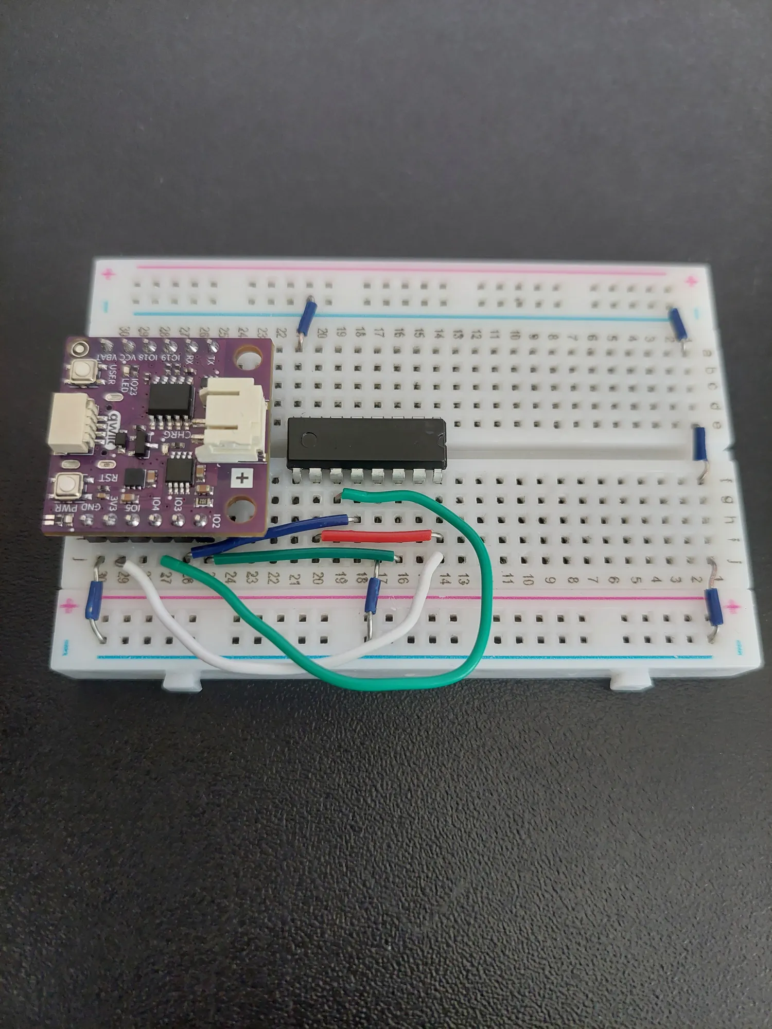
a16 and c16 are the same electrical point, which is how the resistor in the next step reaches the chip pin without a wire.10. First 330 Ω resistor
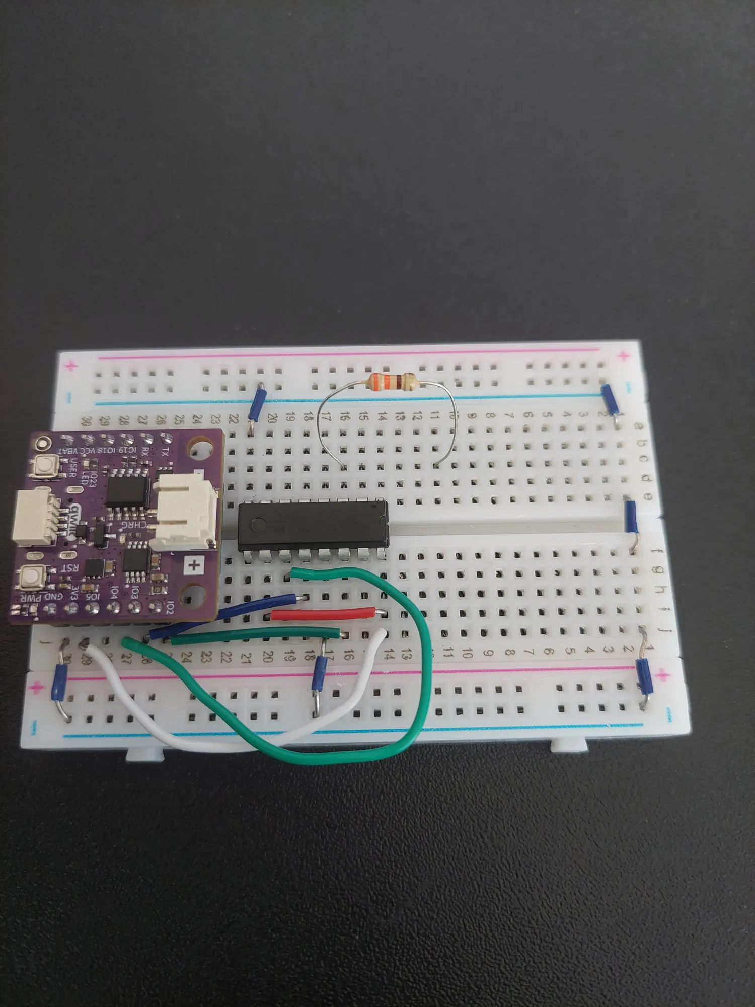
Now the outputs. The first chain starts at Q3, pin 3, on the a–e side at row 16. The resistor reaches the chip pin directly, so this chain is the only one that needs no feed wire: one leg in c16, the other in c11.
11. First LED, bit 3
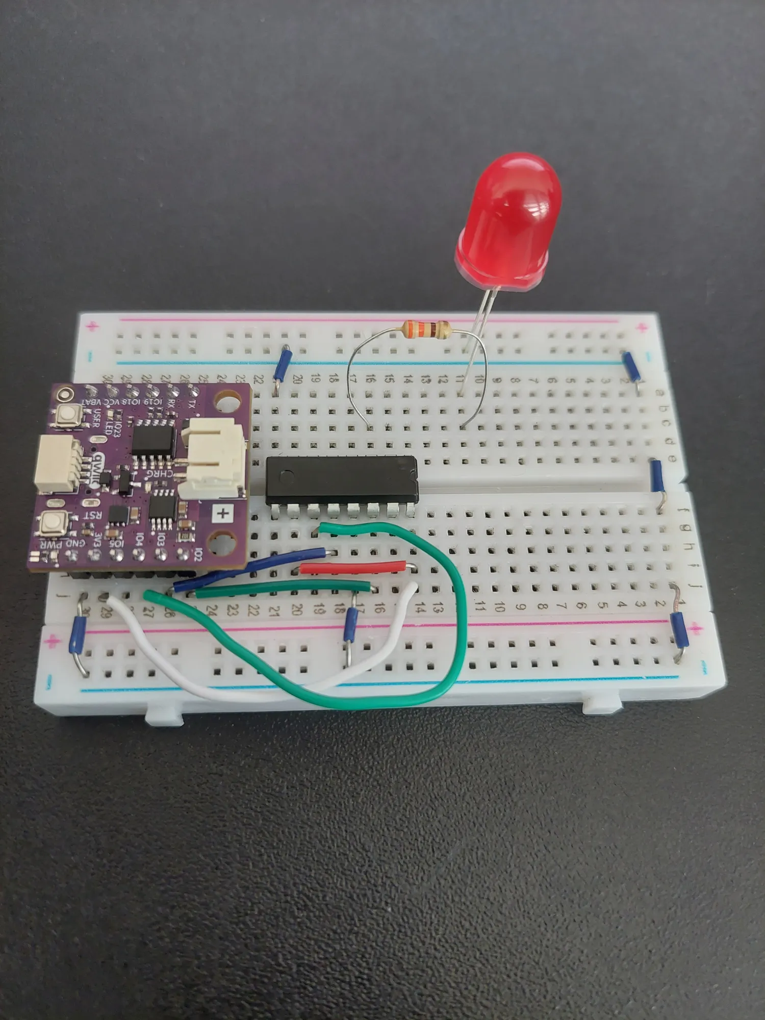
The long leg (anode) goes into a11, the row where the resistor ends. Column a is the outermost one, so the leg is as close to the rail as it can get. The short leg (cathode) bends straight into the top blue − rail, which saves a jumper on every LED in this build.
12. Feed wire for bit 2
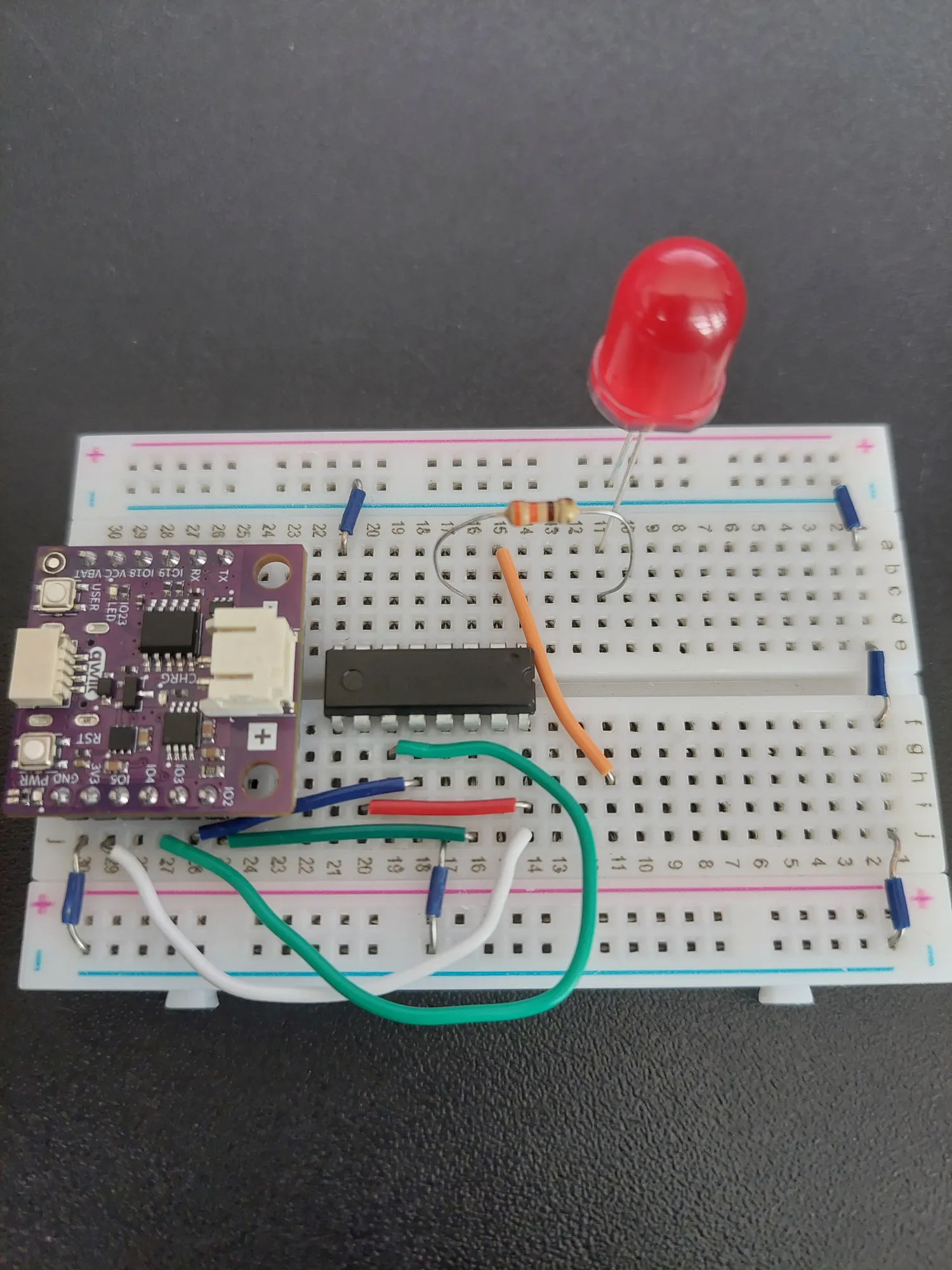
Q2 is pin 2, at a15. Its LED goes on the other side of the channel, so an orange wire carries the output across to h11.
13. Second 330 Ω resistor
From i11 to i8, continuing the chain on the f–j side.
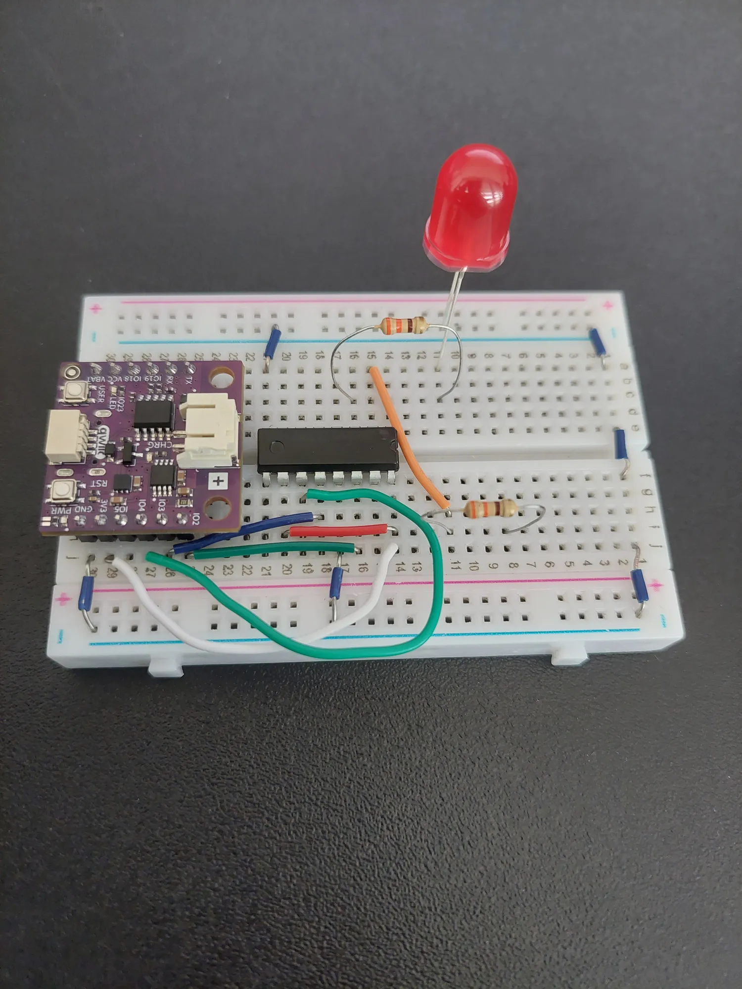
14. Second LED, bit 2
Anode into j8, cathode bent into the bottom blue − rail this time, since this chain lives on the f–j side.
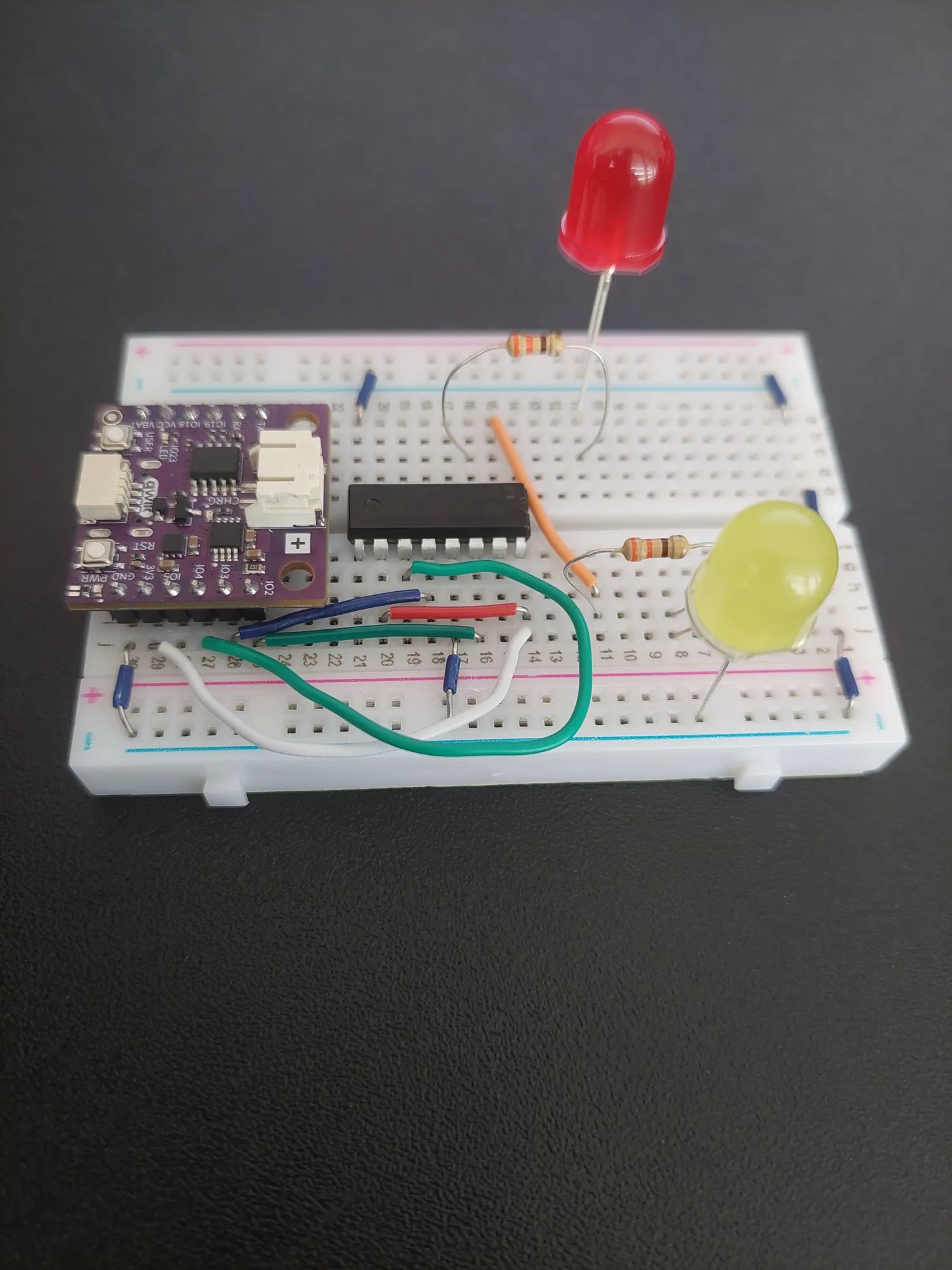
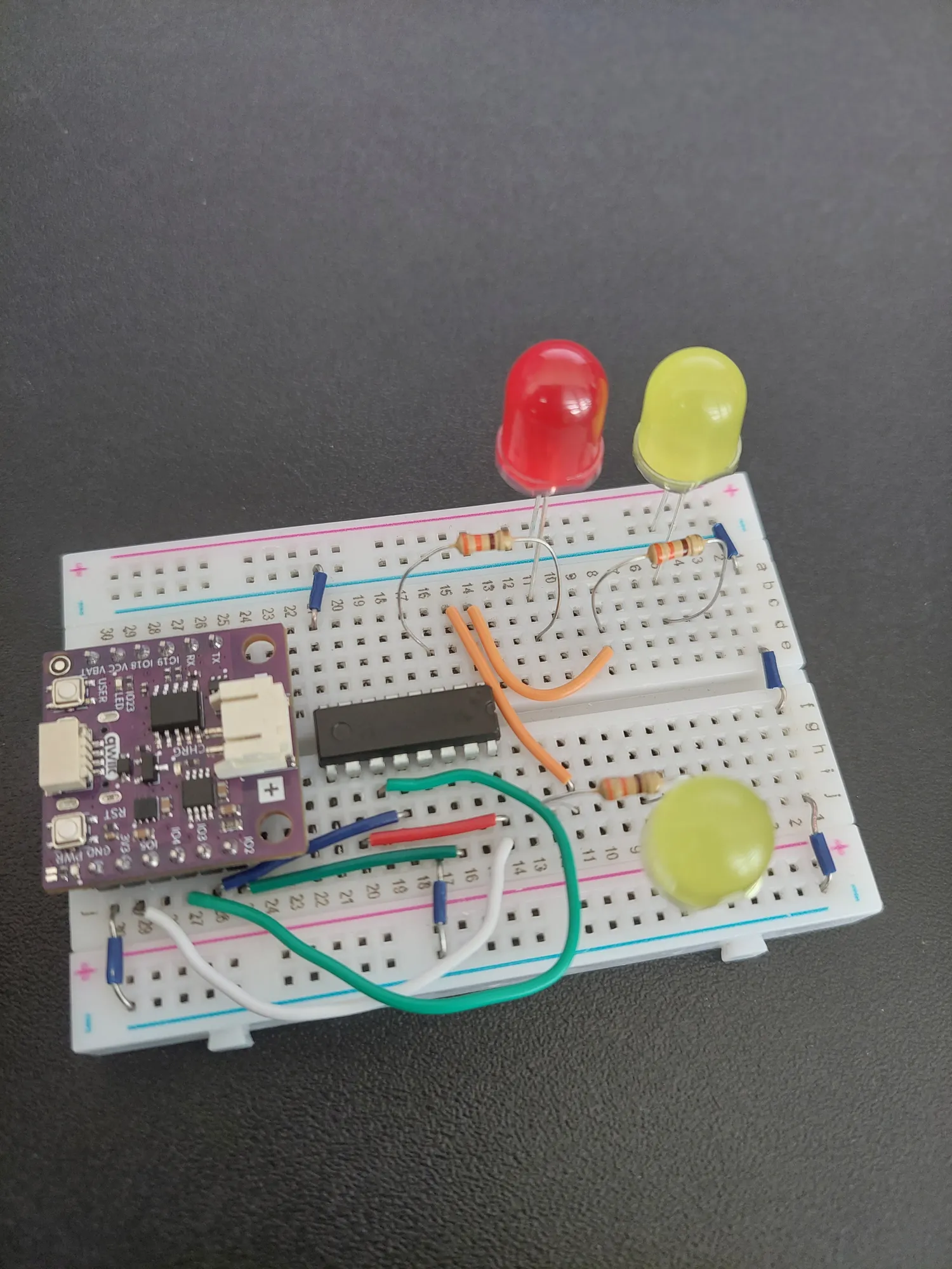
15. Feed wire for bit 1
A second orange wire takes Q1 from a14 to d8, staying on the a–e side.
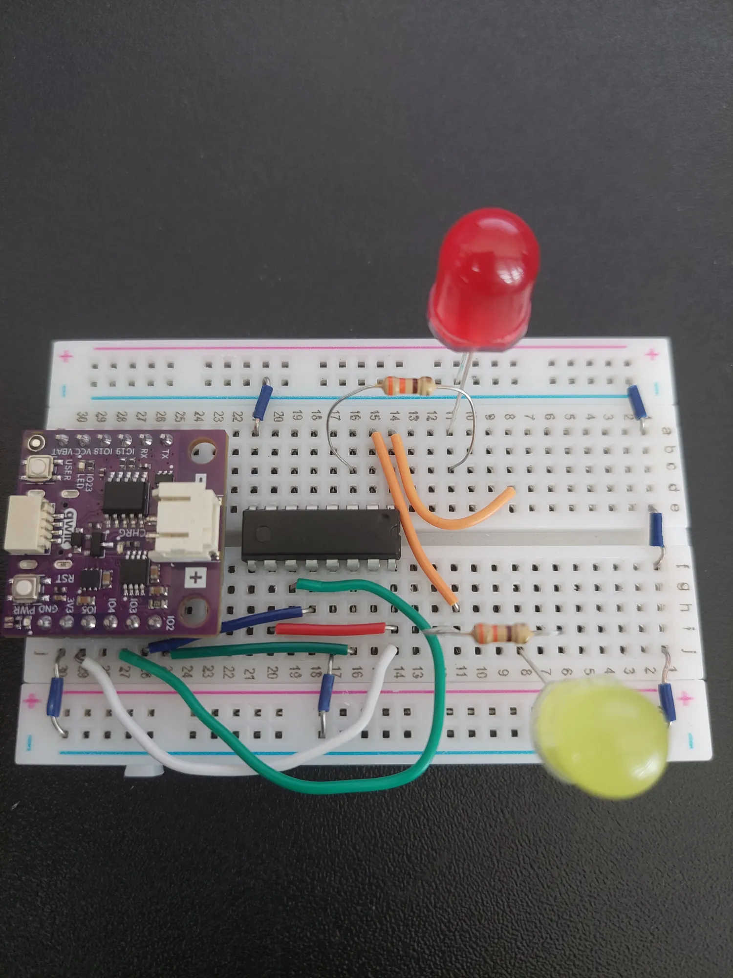
16. Third 330 Ω resistor
From c8 to c5.
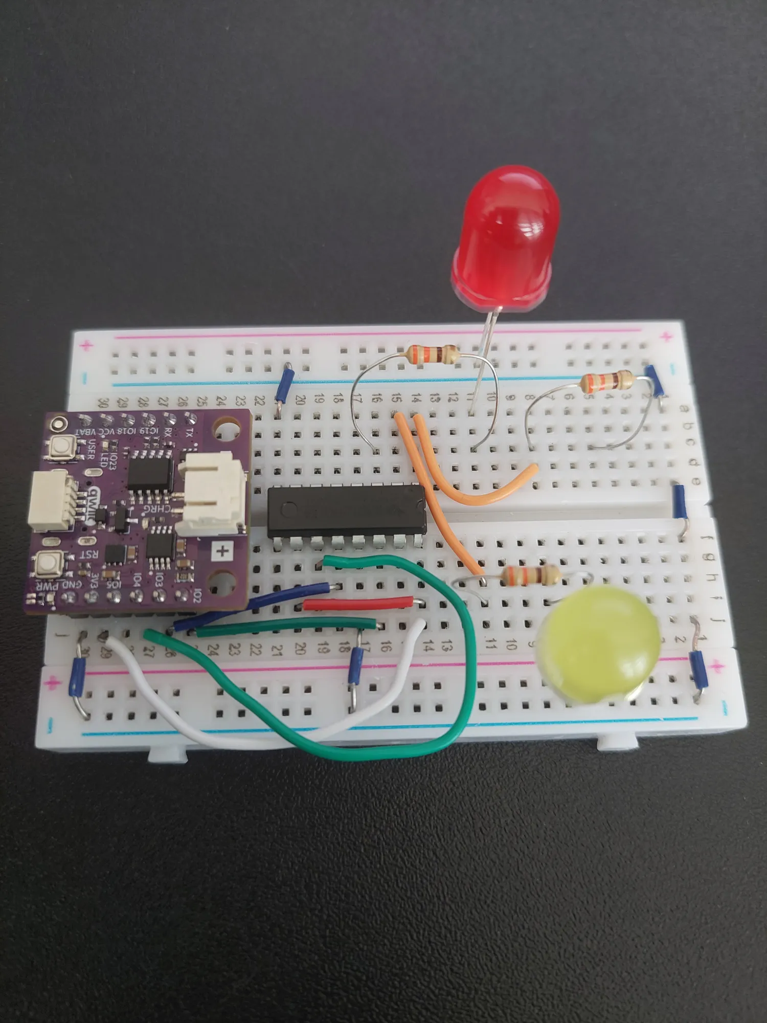
17. Third LED, bit 1
Anode into a5, cathode into the top blue − rail.
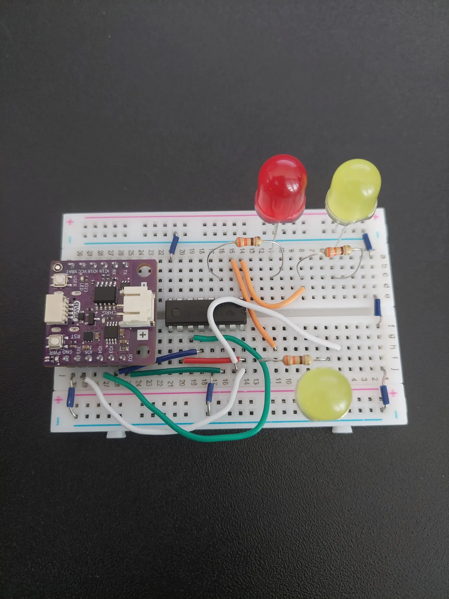
18. Feed wire for bit 0
Q0 is pin 15, on the f–j side at j15, the only output on that side of the chip. A white wire takes it along to h5.
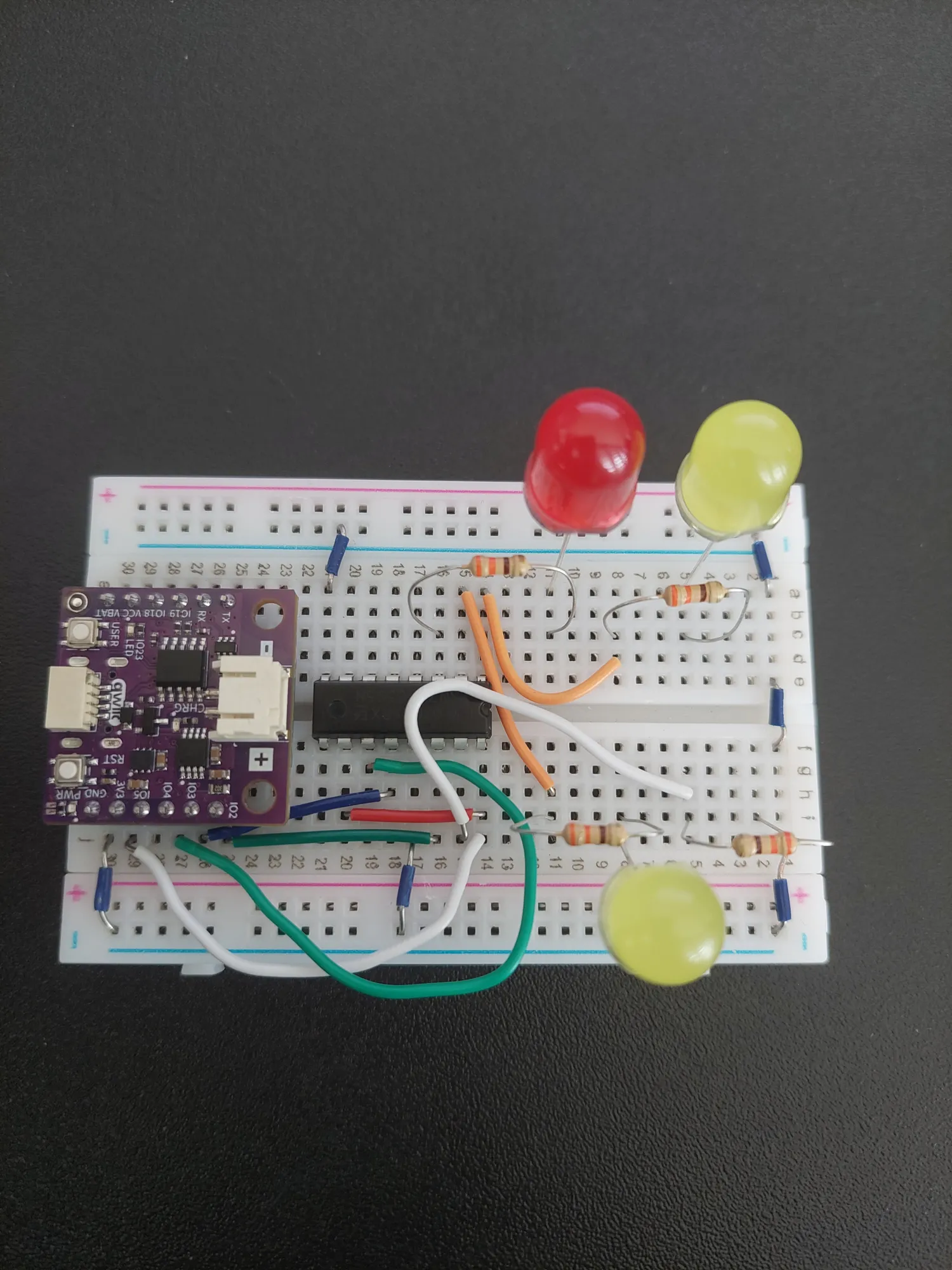
19. Fourth 330 Ω resistor
From i5 to i2, the last one.
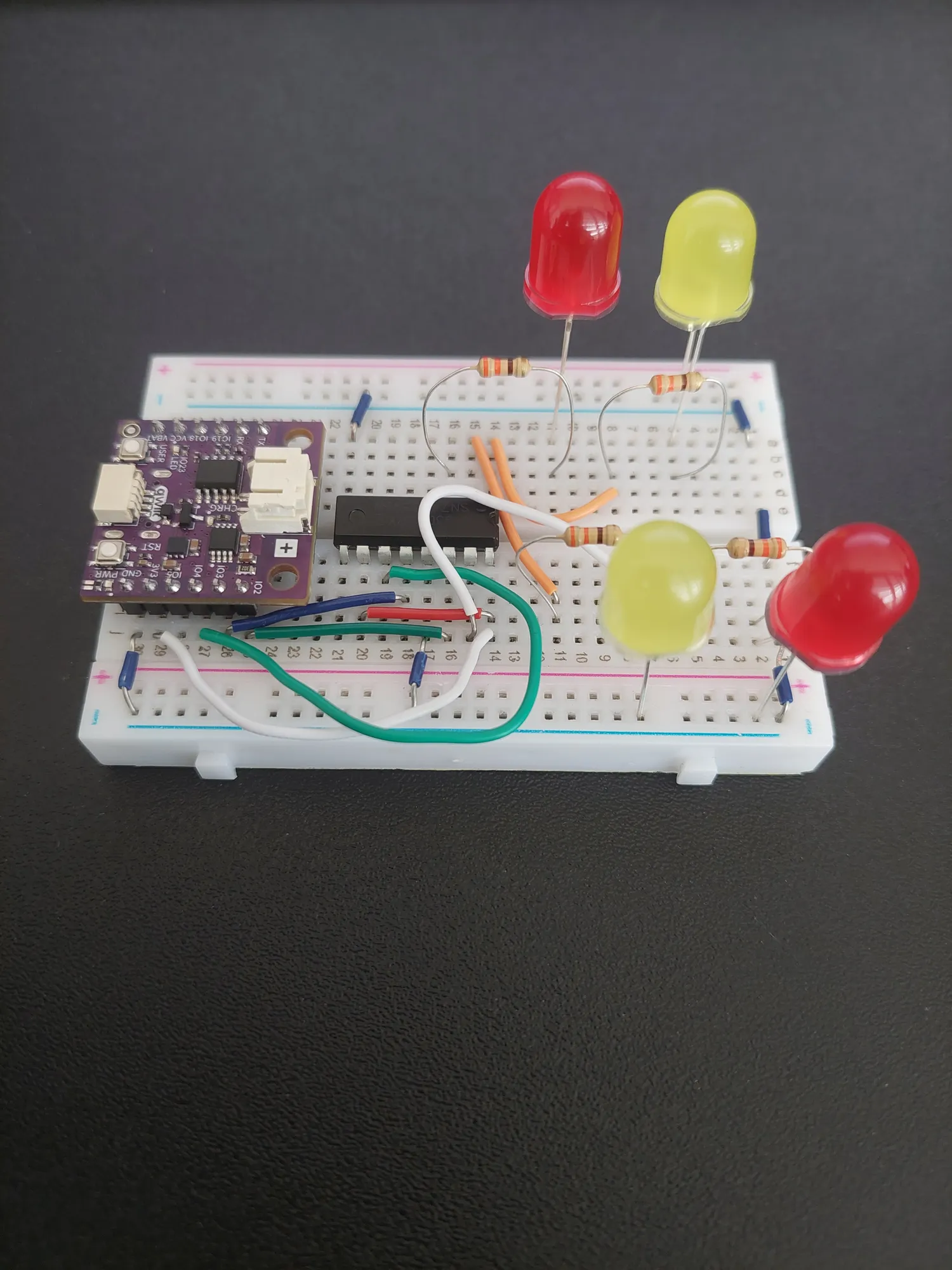
20. Fourth LED, bit 0
Anode into j2, cathode into the bottom blue − rail. All four chains are now in place:
| Bit | Counts | Chip pin | Feed wire | 330 Ω | LED anode | Cathode |
|---|---|---|---|---|---|---|
| 3 | 8 | 3 · Q3 (a16) | none needed | c16 to c11 | a11 | top − rail |
| 2 | 4 | 2 · Q2 (a15) | a15 to h11 | i11 to i8 | j8 | bottom − rail |
| 1 | 2 | 1 · Q1 (a14) | a14 to d8 | c8 to c5 | a5 | top − rail |
| 0 | 1 | 15 · Q0 (j15) | j15 to h5 | i5 to i2 | j2 | bottom − rail |
21. Plug in the USB-C cable
How three pins become eight
A shift register is a row of eight memory cells with a door at one end. DS is the door. Every time the clock pin goes up, whatever is sitting on DS moves into the first cell and every cell passes its contents along to the next one. Eight clock pulses, eight bits stored.
If the outputs changed while that was happening, you would watch the bits stampede across the LEDs on their way to their seats. They do not, because of the third pin. ST_CP, the latch, holds a private copy: the outputs keep showing the previous eight bits until you raise the latch, and then all eight change at the same instant.
That is the whole trick, and it is why the script does the same three things every time round:
- Pull the latch low to stop the outputs changing
- Call
shift_out()to send eight bits, clocking each one in - Pull the latch high to show them all at once
Two more pins have to be told how to behave, and they are the ones people forget. MR (Master Reset) wipes the register whenever it is low, so it is tied high. OE (Output Enable) disconnects the outputs whenever it is high, so it is tied low. Neither is optional: a CMOS input left floating picks up whatever electrical noise is nearby and does as it pleases.
Writing shift_out() yourself
Arduino has a ready-made shiftOut(). MicroPython does not, so the script includes its own, and it is worth reading, because it is the clearest look at bit manipulation in the whole kit:
def shift_out(value):
    for i in range(7, -1, -1):
        bit = (value >> i) & 1
        data_pin.value(bit)
        clock_pin.value(1)
        clock_pin.value(0)
Three ideas are doing all the work:
range(7, -1, -1)counts down: 7, 6, 5, … 1, 0. The three numbers are start, stop and step, and the stop is never included, which is why it ends at-1to reach 0. Counting down is what sends the most significant bit first, which is the order the 74HC595 expects.value >> iis a right shift: it moves every bit of the numberiplaces to the right, so the bit we care about ends up at the bottom.& 1is a bitwise AND with1, which keeps only that bottom bit and discards everything above it.
Put together, (value >> i) & 1 reads out bit number i of the value, on its own, as a 0 or a 1. Setting data_pin to it and then pulsing the clock up and down is one bit delivered.
Why only four LEDs? The chip has eight outputs, but counter & 0x0F keeps the value inside four bits, so Q4 to Q7 are always zero. 0x0F is 15, which in binary is 1111; combining any number with 1111 this way keeps its lowest four bits and throws the rest away. Pin 9 (Q7') is the spare bit falling out of the far end. That is what you would wire to the DS of a second chip to chain two registers into sixteen outputs.
counter = (counter + 1) % 16 is the same wrap-round trick as the alarm clock uses for hours and minutes. % gives the remainder, so 16 becomes 0 and the counter starts again.Code
from machine import Pin
import time

# This is a variable to which we pass the number of pin that we had connected the data pin of the shift register to,
# marked DS on the chip. This is the pin the bits themselves travel over, one after another.
#
# Remember that each of the four LEDs on the shift register outputs needs its own 330 Ohm resistor in series with it,
# exactly as if it were wired straight to the board.
DATA_PIN = 2

# This is a variable to which we pass the number of pin that we had connected the latch pin of the shift register to.
# On the 74HC595 chip this pin is marked ST_CP. The latch is what tells the chip "the data I sent you is complete,
# show it now", which is why the LEDs change all at once instead of flickering through every step.
LATCH_PIN = 3

# This is a variable to which we pass the number of pin that we had connected the clock pin of the shift register to,
# marked SH_CP on the chip. The clock is a pin we switch up and down, and every time it goes up the chip takes in one
# more bit.
CLOCK_PIN = 4

# Here we create our three Pin objects. Pin.OUT tells the board that these pins should write a value instead of
# reading one, since all three of them send information to the chip.
data_pin = Pin(DATA_PIN, Pin.OUT)
latch_pin = Pin(LATCH_PIN, Pin.OUT)
clock_pin = Pin(CLOCK_PIN, Pin.OUT)

# Start with all three pins low, so the chip begins from a known state.
data_pin.value(0)
latch_pin.value(0)
clock_pin.value(0)

# This variable holds the value of our counter. Each pass through the loop it grows by one, and after 15 it starts
# over from zero.
counter = 0


def shift_out(value):
    # This is a function we wrote ourselves, because there is no ready-made function for shifting a byte out.
    # It sends one byte out over the data pin, one bit at a time, pulsing the clock pin after each bit.
    # range(7, -1, -1) counts down from 7 to 0, so we start with the most significant bit, meaning the leftmost one,
    # which is the order the 74HC595 expects.
    # Shifting the value right by i positions and combining it with 1 using the bitwise AND ("&") is how we pick out
    # the single bit we want to send.
    for i in range(7, -1, -1):
        bit = (value >> i) & 1
        data_pin.value(bit)
        clock_pin.value(1)
        clock_pin.value(0)


while True:

    # Here we keep our counter inside four bits. The "&" is a bitwise AND, and 0x0F is the hexadecimal way of writing
    # the number 15, which in binary is 1111. Combining a number with 1111 this way keeps only its lowest four bits.
    value = counter & 0x0F

    # Pulling the latch pin low tells the chip that we are about to send new data and that it should not change its
    # outputs yet. Without this the LEDs would visibly flicker while the bits are still arriving.
    latch_pin.value(0)

    # Send the eight bits of our value to the chip, using our own function above.
    shift_out(value)

    # Pulling the latch pin back high tells the chip that the data is complete. Only now do the outputs change, and
    # all eight of them change together.
    latch_pin.value(1)

    # Print the value too, so you can compare the number with the pattern of lit LEDs.
    print(value)

    # Count one up, and start over from zero once we pass 15, because four LEDs cannot show any number higher than
    # that. The "%" operator gives the remainder of a division, which is a short way of wrapping a counter around.
    counter = (counter + 1) % 16

    # time.sleep() starts a pause in the code, given in seconds. Half a second is slow enough to follow the counting
    # with your eyes. Feel free to experiment with this value.
    time.sleep(0.5)
What you should see
The four LEDs count from 0 to 15 and start again. Each number is held for half a second, so one full lap takes eight seconds.
Reading a number off the LEDs is a matter of adding up the ones that are lit. Along the board, away from the chip, the four are worth 8, 4, 2 and 1. So one LED on its own at the far end is 1; the two nearest the chip together are 8 + 4 = 12; all four lit is 15, the largest number four LEDs can show, and the next step after that is back to 0.
Unlike the Arduino version of this project, the script also prints each number as it displays it, so you can check the LEDs against the count:
0
1
2
3
4
5
Watch the 1 LED for a while and you will see the pattern that makes binary counting work: it changes every single step. The 2 changes half as often, the 4 half as often again, and the 8 only twice in the whole lap. Each LED flips at exactly half the rate of the one before it. The printed column shows the same thing in numbers.
If nothing lights up at all, unplug the USB cable and check the notch on the chip first. A 74HC595 seated the wrong way round is by far the most common cause, and it is worth catching quickly: turning the chip end for end swaps rows 14 and 21 across the channel, so the 3V3 wire lands on pin 8 (GND) and the ground jumper lands on pin 16 (VCC). The chip then has its supply backwards rather than absent, which forward-biases the diode inside it that is normally reverse-biased. It will not work, it may get noticeably warm, and it can be damaged for good, so do not leave it powered while you work out what is wrong. If the LEDs are lit but never change, the clock or latch wire is in the wrong row; the console counting up while the LEDs sit still proves the fault is in the wiring and not the code. If one LED never lights, its own chain is at fault, and the other three prove the chip is fine.
Full example
Check out the full example code on the link below:
7.5_Shift_Register.py
Project demonstrating how to use a 74HC595 shift register to control four LEDs as a 4-bit binary counter using only three NULA MINI pins.